- 您现在的位置:买卖IC网 > PDF目录192306 > S71PL129JC0BFW9Z2 (SPANSION LLC) Stacked Multi-Chip Product (MCP) Flash Memory PDF资料下载
参数资料
| 型号: | S71PL129JC0BFW9Z2 |
| 厂商: | SPANSION LLC |
| 元件分类: | 存储器 |
| 英文描述: | Stacked Multi-Chip Product (MCP) Flash Memory |
| 中文描述: | SPECIALTY MEMORY CIRCUIT, PBGA64 |
| 封装: | 8 X 11.60 MM, 1.20 MM HEIGHT, LEAD FREE, FBGA-64 |
| 文件页数: | 106/153页 |
| 文件大小: | 3651K |
| 代理商: | S71PL129JC0BFW9Z2 |
第1页第2页第3页第4页第5页第6页第7页第8页第9页第10页第11页第12页第13页第14页第15页第16页第17页第18页第19页第20页第21页第22页第23页第24页第25页第26页第27页第28页第29页第30页第31页第32页第33页第34页第35页第36页第37页第38页第39页第40页第41页第42页第43页第44页第45页第46页第47页第48页第49页第50页第51页第52页第53页第54页第55页第56页第57页第58页第59页第60页第61页第62页第63页第64页第65页第66页第67页第68页第69页第70页第71页第72页第73页第74页第75页第76页第77页第78页第79页第80页第81页第82页第83页第84页第85页第86页第87页第88页第89页第90页第91页第92页第93页第94页第95页第96页第97页第98页第99页第100页第101页第102页第103页第104页第105页当前第106页第107页第108页第109页第110页第111页第112页第113页第114页第115页第116页第117页第118页第119页第120页第121页第122页第123页第124页第125页第126页第127页第128页第129页第130页第131页第132页第133页第134页第135页第136页第137页第138页第139页第140页第141页第142页第143页第144页第145页第146页第147页第148页第149页第150页第151页第152页第153页
54
S71PL129JC0/S71PL129JB0/S71PL129JA0
S71PL129Jxx_00_A8 October 28, 2005
Advance
Info rmation
DYB to a 1 protects the sector from programs or erases. Since this is a volatile
bit, removing power or resetting the device will clear the DYBs. The bank address
is latched when the command is written.
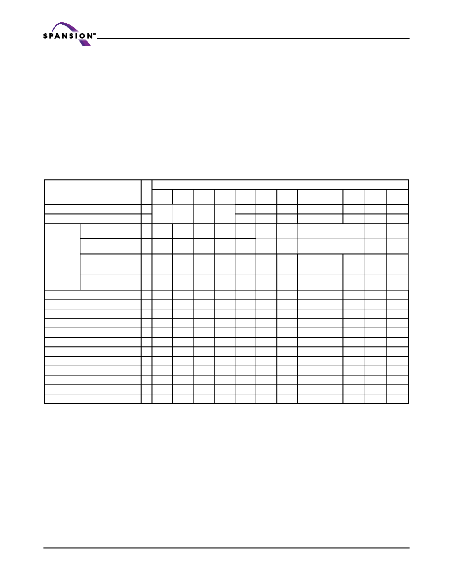
Command
The programming of either the PPB or DYB for a given sector or sector group can
be verified by writing a Sector Protection Status command to the device.
Note that there is no single command to independently verify the programming
of a DYB for a given sector group.
Command Definitions Tables
Legend:
BA = Address of bank switching to autoselect mode, bypass mode, or erase operation. Determined by Amax:A19.
PA = Program Address (Amax:A0). Addresses latch on falling edge of WE# or CE1#/CE2# pulse, whichever happens
later.
PD = Program Data (DQ15:DQ0) written to location PA. Data latches on rising edge of WE# or CE1#/CE2# pulse,
whichever happens first.
RA = Read Address (Amax:A0).
RD = Read Data (DQ15:DQ0) from location RA.
SA = Sector Address (Amax:A12) for verifying (in autoselect mode) or erasing.
WD = Write Data. See “Configuration Register” definition for specific write data. Data latched on rising edge of WE#.
X = Don’t care
Notes:
1. See Table 1 for description of bus operations.
2. All values are in hexadecimal.
3. Shaded cells in table denote read cycles. All other cycles are write operations.
Table 12. Memory Array Command Definitions
Command (Notes)
Cy
cle
s
Addr
Data
Addr
Data
Addr
Data
Addr
Data
Addr
Data
Addr
Data
Read (Note 5)
1
RA
RD
Reset (Note 6)
1
XXX
F0
Autoselect
Manufacturer ID
4
555
AA
2AA
55
(BA)
555
90
(BA)
X00
01
Device ID (Note 10)
6
555
AA
2AA
55
(BA)
555
90
(BA)
X01
227E
(BA)
X0E
(BA)
X0F
Secured Silicon Sector
Factory Protect (Note
4
555
AA
2AA
55
(BA)
555
90
X03
Sector Group Protect
Verify (Note 9)
4
555
AAA
2AA
55
(BA)
555
90
(SA)
X02
XX00/
XX01
Program
4
555
AA
2AA
55
555
A0
PA
PD
Chip Erase
6
555
AA
2AA
55
555
80
555
AA
2AA
55
555
10
Sector Erase
6
555
AA
2AA
55
555
80
555
AA
2AA
55
SA
30
Program/Erase Suspend (Note 11)
1
BA
B0
Program/Erase Resume (Note 12)
1
BA
30
CFI Query (Note 13)
1
55
98
Accelerated Program (Note 15)
2
XX
A0
PA
PD
Unlock Bypass Entry (Note 15)
3
555
AA
2AA
55
555
20
Unlock Bypass Program (Note 15)
2
XX
A0
PA
PD
Unlock Bypass Erase (Note 15)
2
XX
80
XX
10
Unlock Bypass CFI (Notes 13, 15)
1
XX
98
Unlock Bypass Reset (Note 15)
2
XXX
90
XXX
00
相关PDF资料 |
PDF描述 |
|---|---|
| S71PL129NC0HFW4U3 | SPECIALTY MEMORY CIRCUIT, PBGA64 |
| S71PL191HB0BFI100 | SPECIALTY MEMORY CIRCUIT, PBGA73 |
| S71VS128RC0ZHK203 | SPECIALTY MEMORY CIRCUIT, PBGA56 |
| S71VS128RC0ZHK2L2 | SPECIALTY MEMORY CIRCUIT, PBGA56 |
| S71WS512ND0BAWEH | SPECIALTY MEMORY CIRCUIT, PBGA84 |
相关代理商/技术参数 |
参数描述 |
|---|---|
| S71PL129JC0BFW9Z3 | 制造商:SPANSION 制造商全称:SPANSION 功能描述:Stacked Multi-Chip Product (MCP) Flash Memory |
| S71PL129N | 制造商:SPANSION 制造商全称:SPANSION 功能描述:256/128/128兆位(16/8/8米x16位元)的CMOS 3.0电压只有同时读/写,页面模式闪存 |
| S71PL129NB0 | 制造商:SPANSION 制造商全称:SPANSION 功能描述:MirrorBit MCPs |
| S71PL129NB0HAW5B0 | 制造商:SPANSION 制造商全称:SPANSION 功能描述:MirrorBit MCPs |
| S71PL129NB0HAW5B2 | 制造商:SPANSION 制造商全称:SPANSION 功能描述:MirrorBit MCPs |
发布紧急采购,3分钟左右您将得到回复。