- 您现在的位置:买卖IC网 > PDF目录192306 > S71PL129JC0BFW9Z2 (SPANSION LLC) Stacked Multi-Chip Product (MCP) Flash Memory PDF资料下载
参数资料
| 型号: | S71PL129JC0BFW9Z2 |
| 厂商: | SPANSION LLC |
| 元件分类: | 存储器 |
| 英文描述: | Stacked Multi-Chip Product (MCP) Flash Memory |
| 中文描述: | SPECIALTY MEMORY CIRCUIT, PBGA64 |
| 封装: | 8 X 11.60 MM, 1.20 MM HEIGHT, LEAD FREE, FBGA-64 |
| 文件页数: | 58/153页 |
| 文件大小: | 3651K |
| 代理商: | S71PL129JC0BFW9Z2 |
第1页第2页第3页第4页第5页第6页第7页第8页第9页第10页第11页第12页第13页第14页第15页第16页第17页第18页第19页第20页第21页第22页第23页第24页第25页第26页第27页第28页第29页第30页第31页第32页第33页第34页第35页第36页第37页第38页第39页第40页第41页第42页第43页第44页第45页第46页第47页第48页第49页第50页第51页第52页第53页第54页第55页第56页第57页当前第58页第59页第60页第61页第62页第63页第64页第65页第66页第67页第68页第69页第70页第71页第72页第73页第74页第75页第76页第77页第78页第79页第80页第81页第82页第83页第84页第85页第86页第87页第88页第89页第90页第91页第92页第93页第94页第95页第96页第97页第98页第99页第100页第101页第102页第103页第104页第105页第106页第107页第108页第109页第110页第111页第112页第113页第114页第115页第116页第117页第118页第119页第120页第121页第122页第123页第124页第125页第126页第127页第128页第129页第130页第131页第132页第133页第134页第135页第136页第137页第138页第139页第140页第141页第142页第143页第144页第145页第146页第147页第148页第149页第150页第151页第152页第153页
148
S71PL129JC0/S71PL129JB0/S71PL129JA0
S71PL129Jxx_00_A8 October 28, 2005
Advance
Info rmation
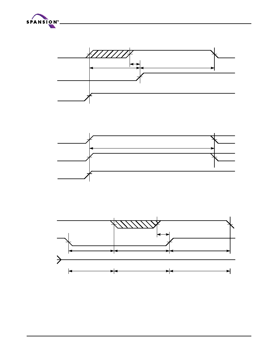
Read/Write Timings
Notes:
1. The tC2LH specifies after VDD reaches specified minimum level.
2. For 32M only: The minimum and maximum VDD transition time from 0 V to specified VDD minimum are 30 s and 50 ms respectively.
Figure 69. Power-up Timing #1
Notes:
1. The tCHH specifies after VDD reaches specified minimum level and applicable to both CE1# and CE2.
2. For 32M only: The minimum and maximum VDD transition time from 0 V to specified VDD minimum are 30 s and 50 ms respectively. If
transition time of VDD (from 0 V to VDD min.) is longer than 50 ms, POWER-UP Timing #1 must be applied.
Figure 70. Power-up Timing #2
Note: This Power Down mode can be also used as a reset timing if POWER-UP timing above could not be satisfied and
Power-Down program was not performed prior to this reset.
Figure 71. Power Down Entry and Exit Timing
tC2LH
CE1#
VDD
VDD min
0V
CE2
tCHH
tCHS
CE1#
VDD
VDD min
0V
CE2
tCHH
tCSP
CE1#
Power Down Entry
CE2
tC2LP
tCHH (tCHHP)
Power Down Mode
Power Down Exit
tCHS
DQ
High-Z
相关PDF资料 |
PDF描述 |
|---|---|
| S71PL129NC0HFW4U3 | SPECIALTY MEMORY CIRCUIT, PBGA64 |
| S71PL191HB0BFI100 | SPECIALTY MEMORY CIRCUIT, PBGA73 |
| S71VS128RC0ZHK203 | SPECIALTY MEMORY CIRCUIT, PBGA56 |
| S71VS128RC0ZHK2L2 | SPECIALTY MEMORY CIRCUIT, PBGA56 |
| S71WS512ND0BAWEH | SPECIALTY MEMORY CIRCUIT, PBGA84 |
相关代理商/技术参数 |
参数描述 |
|---|---|
| S71PL129JC0BFW9Z3 | 制造商:SPANSION 制造商全称:SPANSION 功能描述:Stacked Multi-Chip Product (MCP) Flash Memory |
| S71PL129N | 制造商:SPANSION 制造商全称:SPANSION 功能描述:256/128/128兆位(16/8/8米x16位元)的CMOS 3.0电压只有同时读/写,页面模式闪存 |
| S71PL129NB0 | 制造商:SPANSION 制造商全称:SPANSION 功能描述:MirrorBit MCPs |
| S71PL129NB0HAW5B0 | 制造商:SPANSION 制造商全称:SPANSION 功能描述:MirrorBit MCPs |
| S71PL129NB0HAW5B2 | 制造商:SPANSION 制造商全称:SPANSION 功能描述:MirrorBit MCPs |
发布紧急采购,3分钟左右您将得到回复。