- 您现在的位置:买卖IC网 > PDF目录192306 > S71PL129JC0BFW9Z2 (SPANSION LLC) Stacked Multi-Chip Product (MCP) Flash Memory PDF资料下载
参数资料
| 型号: | S71PL129JC0BFW9Z2 |
| 厂商: | SPANSION LLC |
| 元件分类: | 存储器 |
| 英文描述: | Stacked Multi-Chip Product (MCP) Flash Memory |
| 中文描述: | SPECIALTY MEMORY CIRCUIT, PBGA64 |
| 封装: | 8 X 11.60 MM, 1.20 MM HEIGHT, LEAD FREE, FBGA-64 |
| 文件页数: | 47/153页 |
| 文件大小: | 3651K |
| 代理商: | S71PL129JC0BFW9Z2 |
第1页第2页第3页第4页第5页第6页第7页第8页第9页第10页第11页第12页第13页第14页第15页第16页第17页第18页第19页第20页第21页第22页第23页第24页第25页第26页第27页第28页第29页第30页第31页第32页第33页第34页第35页第36页第37页第38页第39页第40页第41页第42页第43页第44页第45页第46页当前第47页第48页第49页第50页第51页第52页第53页第54页第55页第56页第57页第58页第59页第60页第61页第62页第63页第64页第65页第66页第67页第68页第69页第70页第71页第72页第73页第74页第75页第76页第77页第78页第79页第80页第81页第82页第83页第84页第85页第86页第87页第88页第89页第90页第91页第92页第93页第94页第95页第96页第97页第98页第99页第100页第101页第102页第103页第104页第105页第106页第107页第108页第109页第110页第111页第112页第113页第114页第115页第116页第117页第118页第119页第120页第121页第122页第123页第124页第125页第126页第127页第128页第129页第130页第131页第132页第133页第134页第135页第136页第137页第138页第139页第140页第141页第142页第143页第144页第145页第146页第147页第148页第149页第150页第151页第152页第153页
138
S71PL129JC0/S71PL129JB0/S71PL129JA0
S71PL129Jxx_00_A8 October 28, 2005
Advance
Info rmation
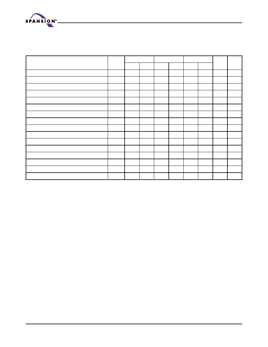
AC Characteristics
Write Operation
Notes:
1. Maximum value is applicable if CE1# is kept at Low without any address change. If the relaxation is needed by system operation, please
contact local Spansion representative for the relaxation of 1s limitation.
2. Minimum value must be equal or greater than the sum of write pulse (tCW, tWP or tBW) and write recovery time (tWR).
3. Write pulse is defined from High to Low transition of CE1#, WE#, or LB#/UB#, whichever occurs last.
4. Applicable for byte mask only. Byte mask setup time is defined to the High to Low transition of CE1# or WE# whichever
occurs last.
5. Applicable for byte mask only. Byte mask hold time is defined from the Low to High transition of CE1# or WE# whichever
occurs first.
6. Write recovery is defined from Low to High transition of CE1#, WE#, or LB#/UB#, whichever occurs first.
7. tWPH minimum is absolute minimum value for device to detect High level. And it is defined at minimum VIH level.
8. If OE# is Low after minimum tOHCL, read cycle is initiated. In other words, OE# must be brought to High within 5ns after
CE1# is brought to Low. Once read cycle is initiated, new write pulse should be input after minimum tRC is met.
9. If OE# is Low after new address input, read cycle is initiated. In other word, OE# must be brought to High at the same time
or before new address valid. Once read cycle is initiated, new write pulse should be input after minimum tRC is met and data
bus is in High-Z.
Parameter
Symbol
16M
32M
64M
Unit
Notes
Min.
Max.
Min.
Max.
Min.
Max.
Write Cycle Time
tWC
70
1000
65
1000
65
1000
ns
1,2
Address Setup Time
tAS
0—0—0—
ns
3
CE1# Write Pulse Width
tCW
45
—
40
—
40
—
ns
3
WE# Write Pulse Width
tWP
45
—
40
—
40
—
ns
3
LB#/UB# Write Pulse Width
tBW
45
—
40
—
40
—
ns
3
LB#/UB# Byte Mask Setup Time
tBS
-5
—
–5
—
–5
—
ns
4
LB#/UB# Byte Mask Hold Time
tBH
-5
—
–5
—
–5
—
ns
5
Write Recovery Time
tWR
0—0—0—
ns
6
CE1# High Pulse Width
tCP
10
—
12
—
12
—
ns
WE# High Pulse Width
tWHP
7.5
1000
7.5
1000
7.5
1000
ns
7
LB#/UB# High Pulse Width
tBHP
10
1000
12
1000
12
1000
ns
Data Setup Time
tDS
15
—
12
—
12
—
ns
Data Hold Time
tDH
0—0—0—
ns
OE# High to CE1# Low Setup Time for Write
tOHCL
-5
—
–5
—
–5
—
ns
8
OE# High to Address Setup Time for Write
tOES
0—0—0—
ns
9
LB# and UB# Write Pulse Overlap
tBWO
30
—
30
—
30
—
ns
相关PDF资料 |
PDF描述 |
|---|---|
| S71PL129NC0HFW4U3 | SPECIALTY MEMORY CIRCUIT, PBGA64 |
| S71PL191HB0BFI100 | SPECIALTY MEMORY CIRCUIT, PBGA73 |
| S71VS128RC0ZHK203 | SPECIALTY MEMORY CIRCUIT, PBGA56 |
| S71VS128RC0ZHK2L2 | SPECIALTY MEMORY CIRCUIT, PBGA56 |
| S71WS512ND0BAWEH | SPECIALTY MEMORY CIRCUIT, PBGA84 |
相关代理商/技术参数 |
参数描述 |
|---|---|
| S71PL129JC0BFW9Z3 | 制造商:SPANSION 制造商全称:SPANSION 功能描述:Stacked Multi-Chip Product (MCP) Flash Memory |
| S71PL129N | 制造商:SPANSION 制造商全称:SPANSION 功能描述:256/128/128兆位(16/8/8米x16位元)的CMOS 3.0电压只有同时读/写,页面模式闪存 |
| S71PL129NB0 | 制造商:SPANSION 制造商全称:SPANSION 功能描述:MirrorBit MCPs |
| S71PL129NB0HAW5B0 | 制造商:SPANSION 制造商全称:SPANSION 功能描述:MirrorBit MCPs |
| S71PL129NB0HAW5B2 | 制造商:SPANSION 制造商全称:SPANSION 功能描述:MirrorBit MCPs |
发布紧急采购,3分钟左右您将得到回复。