- 您现在的位置:买卖IC网 > PDF目录192306 > S71PL129JC0BFW9Z2 (SPANSION LLC) Stacked Multi-Chip Product (MCP) Flash Memory PDF资料下载
参数资料
| 型号: | S71PL129JC0BFW9Z2 |
| 厂商: | SPANSION LLC |
| 元件分类: | 存储器 |
| 英文描述: | Stacked Multi-Chip Product (MCP) Flash Memory |
| 中文描述: | SPECIALTY MEMORY CIRCUIT, PBGA64 |
| 封装: | 8 X 11.60 MM, 1.20 MM HEIGHT, LEAD FREE, FBGA-64 |
| 文件页数: | 69/153页 |
| 文件大小: | 3651K |
| 代理商: | S71PL129JC0BFW9Z2 |
第1页第2页第3页第4页第5页第6页第7页第8页第9页第10页第11页第12页第13页第14页第15页第16页第17页第18页第19页第20页第21页第22页第23页第24页第25页第26页第27页第28页第29页第30页第31页第32页第33页第34页第35页第36页第37页第38页第39页第40页第41页第42页第43页第44页第45页第46页第47页第48页第49页第50页第51页第52页第53页第54页第55页第56页第57页第58页第59页第60页第61页第62页第63页第64页第65页第66页第67页第68页当前第69页第70页第71页第72页第73页第74页第75页第76页第77页第78页第79页第80页第81页第82页第83页第84页第85页第86页第87页第88页第89页第90页第91页第92页第93页第94页第95页第96页第97页第98页第99页第100页第101页第102页第103页第104页第105页第106页第107页第108页第109页第110页第111页第112页第113页第114页第115页第116页第117页第118页第119页第120页第121页第122页第123页第124页第125页第126页第127页第128页第129页第130页第131页第132页第133页第134页第135页第136页第137页第138页第139页第140页第141页第142页第143页第144页第145页第146页第147页第148页第149页第150页第151页第152页第153页
20
S71PL129JC0/S71PL129JB0/S71PL129JA0
S71PL129Jxx_00_A8 October 28, 2005
Advance
Info rmation
Random Read (Non-Page Read)
Address access time (tACC) is equal to the delay from stable addresses to valid
output data. The chip enable access time (tCE) is the delay from the stable ad-
dresses and stable CE# to valid data at the output inputs. The output enable
access time is the delay from the falling edge of the OE# to valid data at the out-
put inputs (assuming the addresses have been stable for at least tACC–tOE time).
Page Mode Read
The device is capable of fast page mode read and is compatible with the page
mode Mask ROM read operation. This mode provides faster read access speed for
random locations within a page. Address bits Amax–A3 select an 8 word page,
and address bits A2–A0 select a specific word within that page. This is an asyn-
chronous operation with the microprocessor supplying the specific word location.
The random or initial page access is tACC or tCE and subsequent page read ac-
cesses (as long as the locations specified by the microprocessor falls within that
page) is equivalent to tPACC. When CE1# and CE#2 are deasserted (=VIH), the
reassertion of CE1# or CE#2 for subsequent access has access time of tACC or
tCE. Here again, CE1#/CE#2 selects the device and OE# is the output control and
should be used to gate data to the output inputs if the device is selected. Fast
page mode accesses are obtained by keeping Amax–A3 constant and changing
A2–A0 to select the specific word within that page.
Simultaneous Read/Write Operation
In addition to the conventional features (read, program, erase-suspend read, and
erase-suspend program), the device is capable of reading data from one bank of
memory while a program or erase operation is in progress in another bank of
memory (simultaneous operation). The bank can be selected by bank addresses
(A21–A19) with zero latency.
The simultaneous operation can execute multi-function mode in the same bank.
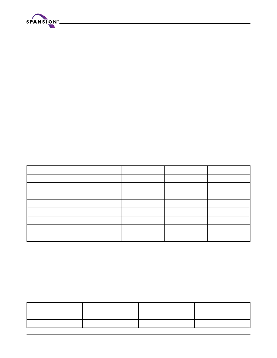
Table 2. Page Select
Word
A2
A1
A0
Word 0
0
Word 1
0
1
Word 2
0
1
0
Word 3
0
1
Word 4
1
0
Word 5
1
0
1
Word 6
1
0
Word 7
1
Bank
CE1#
CE2#
PL129J: A21–A20
Bank 1A
0
1
00
Bank 1B
0
1
01, 10, 11
相关PDF资料 |
PDF描述 |
|---|---|
| S71PL129NC0HFW4U3 | SPECIALTY MEMORY CIRCUIT, PBGA64 |
| S71PL191HB0BFI100 | SPECIALTY MEMORY CIRCUIT, PBGA73 |
| S71VS128RC0ZHK203 | SPECIALTY MEMORY CIRCUIT, PBGA56 |
| S71VS128RC0ZHK2L2 | SPECIALTY MEMORY CIRCUIT, PBGA56 |
| S71WS512ND0BAWEH | SPECIALTY MEMORY CIRCUIT, PBGA84 |
相关代理商/技术参数 |
参数描述 |
|---|---|
| S71PL129JC0BFW9Z3 | 制造商:SPANSION 制造商全称:SPANSION 功能描述:Stacked Multi-Chip Product (MCP) Flash Memory |
| S71PL129N | 制造商:SPANSION 制造商全称:SPANSION 功能描述:256/128/128兆位(16/8/8米x16位元)的CMOS 3.0电压只有同时读/写,页面模式闪存 |
| S71PL129NB0 | 制造商:SPANSION 制造商全称:SPANSION 功能描述:MirrorBit MCPs |
| S71PL129NB0HAW5B0 | 制造商:SPANSION 制造商全称:SPANSION 功能描述:MirrorBit MCPs |
| S71PL129NB0HAW5B2 | 制造商:SPANSION 制造商全称:SPANSION 功能描述:MirrorBit MCPs |
发布紧急采购,3分钟左右您将得到回复。