参数资料
| 型号: | W25Q64FVSSIG |
| 厂商: | Winbond Electronics |
| 文件页数: | 65/89页 |
| 文件大小: | 0K |
| 描述: | IC SPI FLASH 64MBIT 8SOIC |
| 标准包装: | 90 |
| 系列: | SpiFlash® |
| 格式 - 存储器: | 闪存 |
| 存储器类型: | FLASH |
| 存储容量: | 64M(8M x 8) |
| 速度: | 80MHz |
| 接口: | SPI 串行 |
| 电源电压: | 2.7 V ~ 3.6 V |
| 工作温度: | -40°C ~ 85°C |
| 封装/外壳: | 8-SOIC(0.209",5.30mm 宽) |
| 供应商设备封装: | 8-SOIC |
| 包装: | 管件 |
第1页第2页第3页第4页第5页第6页第7页第8页第9页第10页第11页第12页第13页第14页第15页第16页第17页第18页第19页第20页第21页第22页第23页第24页第25页第26页第27页第28页第29页第30页第31页第32页第33页第34页第35页第36页第37页第38页第39页第40页第41页第42页第43页第44页第45页第46页第47页第48页第49页第50页第51页第52页第53页第54页第55页第56页第57页第58页第59页第60页第61页第62页第63页第64页当前第65页第66页第67页第68页第69页第70页第71页第72页第73页第74页第75页第76页第77页第78页第79页第80页第81页第82页第83页第84页第85页第86页第87页第88页第89页
�� �
�
�W25Q64FV�
�6.2.38�
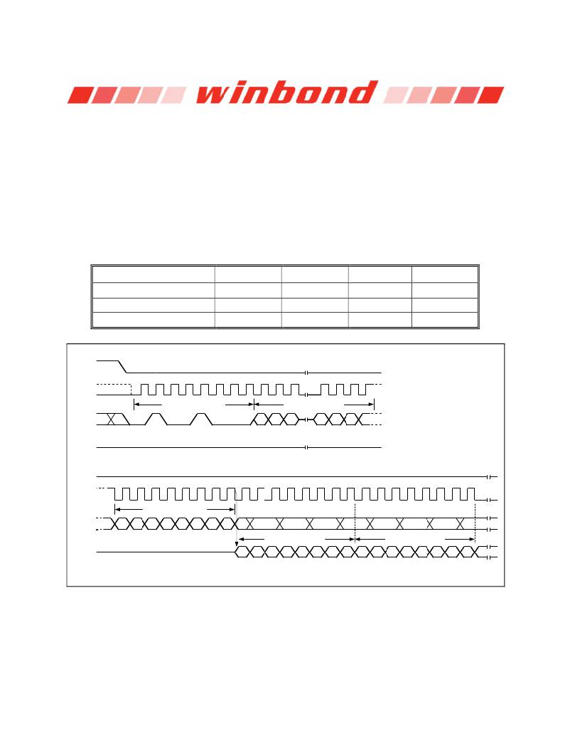
�Read� Security� Registers� (48h)�
�The� Read� Security� Register� instruction� is� similar� to� the� Fast� Read� instruction� and� allows� one� or� more� data�
�bytes� to� be� sequentially� read� from� one� of� the� four� security� registers.� The� instruction� is� initiated� by� driving�
�the� /CS� pin� low� and� then� shifting� the� instruction� code� “48h”� followed� by� a� 24� -bit� address� (A23-A0)� and�
�eight� “dummy”� clocks� into� the� DI� pin.� The� code� and� address� bits� are� latched� on� the� rising� edge� of� the� CLK�
�pin.� After� the� address� is� received,� the� data� byte� of� the� addressed� memory� location� will� be� shifted� out� on�
�the� DO� pin� at� the� falling� edge� of� CLK� with� most� significant� bit� (MSB)� first.� The� byte� address� is�
�automatically� incremented� to� the� next� byte� address� after� each� byte� of� data� is� shifted� out.� Once� the� byte�
�address� reaches� the� last� byte� of� the� register� (byte� FFh),� it� will� reset� to� 00h,� the� first� byte� of� the� register,�
�and� continue� to� increment.� The� instruction� is� completed� by� driving� /CS� high.� The� Read� Security� Register�
�instruction� sequence� is� shown� in� Figure� 37.� If� a� Read� Security� Register� instruction� is� issued� while� an�
�Erase,� Program� or� Write� cycle� is� in� process� (BUSY=1)� the� instruction� is� ignored� and� will� not� have� any�
�effects� on� the� current� cycle.� The� Read� Security� Register� instruction� allows� clock� rates� from� D.C.� to� a�
�maximum� of� F� R� (see� AC� Electrical� Characteristics).�
�ADDRESS�
�Security� Register� #1�
�Security� Register� #2�
�Security� Register� #3�
�A23-16�
�00h�
�00h�
�00h�
�A15-12�
�0001�
�0010�
�0011�
�A11-8�
�0000�
�0000�
�0000�
�A7-0�
�Byte� Address�
�Byte� Address�
�Byte� Address�
�/CS�
�Mode� 3�
�0�
�1�
�2�
�3�
�4�
�5�
�6�
�7�
�8�
�9�
�10�
�28�
�29�
�30�
�31�
�CLK�
�Mode� 0�
�Instruction� (48h)�
�24-Bit� Address�
�DI�
�(IO� 0� )�
�23�
�*�
�22�
�21�
�3�
�2�
�1�
�0�
�DO�
�(IO� 1� )�
�/CS�
�*� =� MSB�
�High� Impedance�
�31�
�32�
�33�
�34�
�35�
�36�
�37�
�38�
�39�
�40�
�41�
�42�
�43�
�44�
�45�
�46�
�47�
�48�
�49�
�50�
�51�
�52�
�53�
�54�
�55�
�CLK�
�Dummy� Byte�
�DI�
�(IO� 0� )�
�0�
�7�
�6�
�5�
�4�
�3�
�2�
�1�
�0�
�Data� Out� 1�
�Data� Out� 2�
�DO�
�(IO� 1� )�
�High� Impedance�
�7�
�*�
�6�
�5�
�4�
�3�
�2�
�1�
�0�
�7�
�*�
�6�
�5�
�4�
�3�
�2�
�1�
�0�
�7�
�Figure� 37.� Read� Security� Registers� Instruction� (SPI� Mode� only)�
�-� 65� -�
�Publication� Release� Date:�
�October� 07,� 2013�
�Revision� L�
�相关PDF资料 |
PDF描述 |
|---|---|
| EP1AGX35DF780I6 | IC ARRIA GX FPGA 35K 780FBGA |
| EP1AGX35DF780I6N | IC ARRIA GX FPGA 35K 780FBGA |
| EP4CE115F23C9L | IC CYCLONE IV FPGA 115K 484-FBGA |
| EP4CE115F23C8 | IC CYCLONE IV FPGA 115K 484-FBGA |
| A3PE3000L-1FG484 | IC FPGA 1KB FLASH 3M 484-FBGA |
相关代理商/技术参数 |
参数描述 |
|---|---|
| W25Q64FVSSIG TR | 制造商:Winbond Electronics Corp 功能描述:SPIFLASH, 64M-BIT, 4KB UNIFORM 制造商:Winbond Electronics Corp 功能描述:IC FLASH 64MBIT 104MHZ 8SOIC 制造商:Winbond 功能描述:SPIFLASH, 64M-BIT, 4KB UNIFORM |
| W25Q64FVSSIG/TRAY | 制造商:Winbond Electronics Corp 功能描述: |
| W25Q64FVSSIP | 制造商:WINBOND 制造商全称:Winbond 功能描述:3V 64M-BIT SERIAL FLASH MEMORY WITH DUAL/QUAD SPI & QPI |
| W25Q64FVTCIG | 制造商:Winbond Electronics Corp 功能描述:64MBIT SPI |
| W25Q64FVTCIP | 制造商:WINBOND 制造商全称:Winbond 功能描述:3V 64M-BIT SERIAL FLASH MEMORY WITH DUAL/QUAD SPI & QPI |
发布紧急采购,3分钟左右您将得到回复。