参数资料
| 型号: | DS3105LN+ |
| 厂商: | Maxim Integrated Products |
| 文件页数: | 77/124页 |
| 文件大小: | 0K |
| 描述: | IC TIMING LINE CARD 64-LQFP |
| 产品培训模块: | Lead (SnPb) Finish for COTS Obsolescence Mitigation Program |
| 标准包装: | 160 |
| 类型: | 定时卡 IC,多路复用器 |
| PLL: | 是 |
| 主要目的: | 以太网,SONET/SDH,Stratum,电信 |
| 输入: | CMOS,LVDS,LVPECL,TTL |
| 输出: | CMOS,LVDS,LVPECL,TTL |
| 电路数: | 1 |
| 比率 - 输入:输出: | 5:2 |
| 差分 - 输入:输出: | 无/是 |
| 频率 - 最大: | 312.5MHz |
| 电源电压: | 1.62 V ~ 1.98 V |
| 工作温度: | -40°C ~ 85°C |
| 安装类型: | 表面贴装 |
| 封装/外壳: | 64-LQFP |
| 供应商设备封装: | 64-LQFP(10x10) |
| 包装: | 托盘 |
第1页第2页第3页第4页第5页第6页第7页第8页第9页第10页第11页第12页第13页第14页第15页第16页第17页第18页第19页第20页第21页第22页第23页第24页第25页第26页第27页第28页第29页第30页第31页第32页第33页第34页第35页第36页第37页第38页第39页第40页第41页第42页第43页第44页第45页第46页第47页第48页第49页第50页第51页第52页第53页第54页第55页第56页第57页第58页第59页第60页第61页第62页第63页第64页第65页第66页第67页第68页第69页第70页第71页第72页第73页第74页第75页第76页当前第77页第78页第79页第80页第81页第82页第83页第84页第85页第86页第87页第88页第89页第90页第91页第92页第93页第94页第95页第96页第97页第98页第99页第100页第101页第102页第103页第104页第105页第106页第107页第108页第109页第110页第111页第112页第113页第114页第115页第116页第117页第118页第119页第120页第121页第122页第123页第124页
DS3105
56
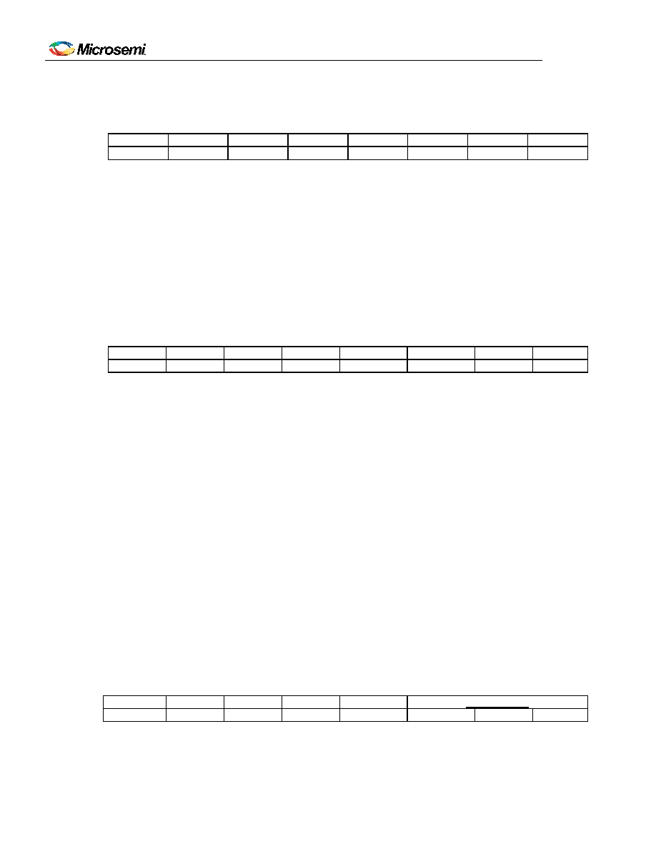
Register Name:
MSR1
Register Description:
Master Status Register 1
Register Address:
05h
Bit #
7
6
5
4
3
2
1
0
Name
—
IC6
IC5
IC4
IC3
—
Default
1
0
1
Bits 5 to 2: Input Clock Status Change (IC[6:3]). Each of these latched status bits is set to 1 when the
corresponding VALSR1 status bit changes state (set or cleared). Each bit is cleared when written with a 1 and not
set again until the VALSR1 bit changes state again. When one of these latched status bits is set, it can cause an
interrupt request on the INTREQ pin if the corresponding interrupt enable bit is set in the IER1 register. See
Section 7.5 for input clock validation/invalidation criteria.
Register Name:
MSR2
Register Description:
Master Status Register 2
Register Address:
06h
Bit #
7
6
5
4
3
2
1
0
Name
STATE
SRFAIL
—
IC9
Default
0
1
Bit 7: T0 DPLL State Change (STATE). This latched status bit is set to 1 when the operating state of the T0 DPLL
changes. STATE is cleared when written with a 1 and not set again until the operating state changes again. When
STATE is set it can cause an interrupt request on the INTREQ pin if the STATE interrupt enable bit is set in the
IER2 register. The current operating state can be read from the T0STATE field of the OPSTATE register. See
Section 7.7.1.
Bit 6: Selected Reference Failed (SRFAIL). This latched status bit is set to 1 when the selected reference to the
T0 DPLL fails, (i.e., no clock edges in two UI). SRFAIL is cleared when written with a 1. When SRFAIL is set it can
cause an interrupt request on the INTREQ pin if the SRFAIL interrupt enable bit is set in the IER2 register. SRFAIL
is not set in free-run mode or holdover mode. See Section 7.5.3.
Bit 0: Input Clock Status Change (IC9). This latched status bit is set to 1 when the corresponding VALSR status
bit changes state (set or cleared). Each bit is cleared when written with a 1 and not set again until the VALSR2 bit
changes state again. When this latched status bit is set it can cause an interrupt request on the INTREQ pin if the
corresponding interrupt enable bit is set in the IER2 register. See Section 7.5 for input clock validation/invalidation
criteria.
Register Name:
FREQ3
Register Description:
Frequency Register 3
Register Address:
07h
Bit #
7
6
5
4
3
2
1
0
Name
—
FREQ[18:16]
Default
0
Bits 2 to 0: Current DPLL Frequency (FREQ[18:16]). See the FREQ1 register description.
相关PDF资料 |
PDF描述 |
|---|---|
| DS3106LN+ | IC TIMING LINE CARD 64-LQFP |
| DS3231MZ+ | IC RTC I2C 8SOIC |
| DS3231SN#T&R | IC RTC W/TCXO 16-SOIC |
| DS3232MZ+ | IC RTC W/SRAM I2C 8SOIC |
| DS3232SN#T&R | IC RTC W/TCXO 20-SOIC |
相关代理商/技术参数 |
参数描述 |
|---|---|
| DS3105LN+ | 功能描述:计时器和支持产品 Line Card Timing IC RoHS:否 制造商:Micrel 类型:Standard 封装 / 箱体:SOT-23 内部定时器数量:1 电源电压-最大:18 V 电源电压-最小:2.7 V 最大功率耗散: 最大工作温度:+ 85 C 最小工作温度:- 40 C 封装:Reel |
| DS3106 | 制造商:MAXIM 制造商全称:Maxim Integrated Products 功能描述:Line Card Timing IC |
| DS3106A10SL3S(621) | 制造商:Amphenol Corporation 功能描述: |
| DS3106A14S2S | 制造商:Amphenol Corporation 功能描述: |
| DS3106A14S2S(621) | 制造商:Amphenol Corporation 功能描述: |
发布紧急采购,3分钟左右您将得到回复。