- 您现在的位置:买卖IC网 > PDF目录295917 > EWIXP455ABT (INTEL CORP) 266 MHz, RISC PROCESSOR, PBGA544 PDF资料下载
参数资料
| 型号: | EWIXP455ABT |
| 厂商: | INTEL CORP |
| 元件分类: | 微控制器/微处理器 |
| 英文描述: | 266 MHz, RISC PROCESSOR, PBGA544 |
| 封装: | LEAD FREE, PLASTIC, BGA-544 |
| 文件页数: | 82/163页 |
| 文件大小: | 1123K |
| 代理商: | EWIXP455ABT |
第1页第2页第3页第4页第5页第6页第7页第8页第9页第10页第11页第12页第13页第14页第15页第16页第17页第18页第19页第20页第21页第22页第23页第24页第25页第26页第27页第28页第29页第30页第31页第32页第33页第34页第35页第36页第37页第38页第39页第40页第41页第42页第43页第44页第45页第46页第47页第48页第49页第50页第51页第52页第53页第54页第55页第56页第57页第58页第59页第60页第61页第62页第63页第64页第65页第66页第67页第68页第69页第70页第71页第72页第73页第74页第75页第76页第77页第78页第79页第80页第81页当前第82页第83页第84页第85页第86页第87页第88页第89页第90页第91页第92页第93页第94页第95页第96页第97页第98页第99页第100页第101页第102页第103页第104页第105页第106页第107页第108页第109页第110页第111页第112页第113页第114页第115页第116页第117页第118页第119页第120页第121页第122页第123页第124页第125页第126页第127页第128页第129页第130页第131页第132页第133页第134页第135页第136页第137页第138页第139页第140页第141页第142页第143页第144页第145页第146页第147页第148页第149页第150页第151页第152页第153页第154页第155页第156页第157页第158页第159页第160页第161页第162页第163页
Functional Overview
Intel IXP45X and Intel IXP46X Product Line of Network Processors Datasheet
May 2005
Document Number: 306261-002
25
In order to limit double-bit errors from occurring, periodically reading the entire usable memory
array will allow the hardware unit within the memory controller to correct any single-bit, ECC
errors that may have occurred prior to these errors becoming double-bit ECC errors. Using this
method is system-dependent.
It is important to note as well, that when sub-word writes (byte writes or half-word writes) to a
32-bit memory with ECC enabled, the memory controller will implement read-modify writes.
Implementing read-modify writes is important to understand when understanding performance
implications when writing software.
To understand a read-modify write, understanding that a byte to be written falls within a 32-bit
word which is addressed on a word-aligned boundary. When a byte write is requested, the memory
controller will read the 32-bit word which encompasses the byte that is to be written. The memory
controller will then modify the specified byte, calculate a new ECC, and then write the entire 32-bit
word back into the memory location it was read from.
The value written back into the memory location will contain the 32-bit word with the modified
byte and the new ECC value.
The MCU supports two banks of DDR SDRAM. The MCU has support for unbuffered DDRI 266
only.
Table 4 illustrates the supported DDR SDRAM configurations for the IXP45X/IXP46X network
processors. The 128/256/512-Mbit, 1-Gbit DDRI SDRAM devices comprise four internal leaves.
The MCU controls the leaf selects within 128/256/512-Mbit, 1-Gbit DDRI SDRAM by toggling
DDRI_BA[0] and DDRI_BA[1].
The two DDR SDRAM chip enables (DDRI_CS[1:0]#) support a DDRI SDRAM memory
subsystem consisting of two banks. The base address for the two contiguous banks are
programmed in the DDR SDRAM Base Register (SDBR) and must be aligned to a 32-Mbyte
boundary. The size of each DDR SDRAM bank is programmed with the DDR SDRAM boundary
registers (SBR0 and SBR1).
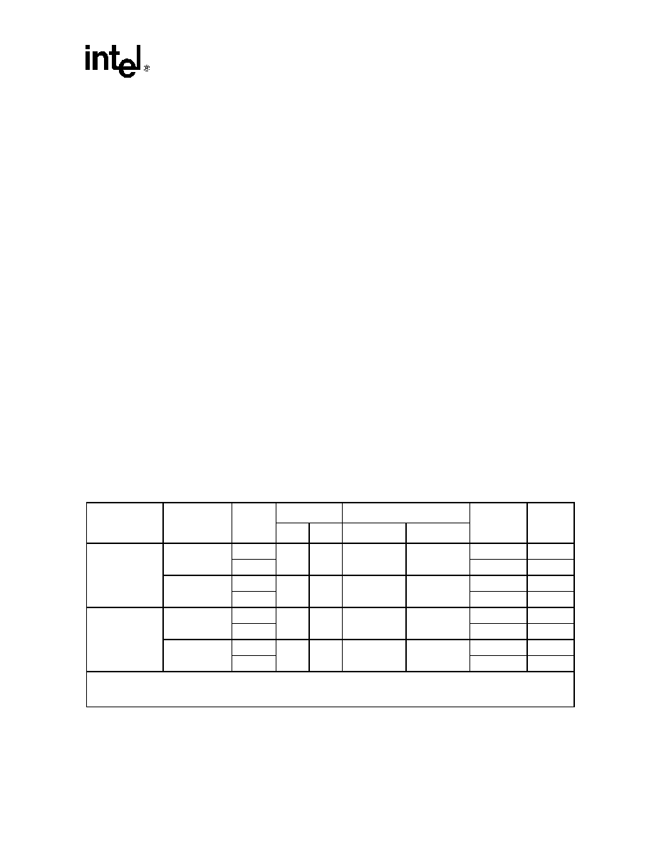
Table 4.
Supported DDRI Memory Configurations (Sheet 1 of 2)
DDRI SDRAM
Technology
DDRI SDRAM
Arrangement
# Banks
Address Size
Leaf Select
Total
Memory
Size1
Page
Size2
Row
Col
DDRI_BA[1]
DDRI_BA[0]
128 Mbit
16M x 8
1
12
10
I_AD[26]
I_AD[25]
64 Mbyte
4K
2
128 Mbyte
4K
8M x 16
1
12
9
I_AD[25]
I_AD[24]
32 Mbyte
2K
2
64 Mbyte
2K
256 Mbit
32M x 8
1
13
10
I_AD[27]
I_AD[26]
128 Mbyte
4K
2
256 Mbyte
4K
16M x 16
1
13
9
I_AD[26]
I_AD[25]
64 Mbyte
2K
2
128 Mbyte
2K
NOTES:
1. Table indicates 32-bit-wide memory subsystem sizes
2. Table indicates 32-bit-wide memory page sizes
相关PDF资料 |
PDF描述 |
|---|---|
| EX5-R-PL | 16 CONTACT(S), MALE, COMBINATION LINE CONNECTOR, SOLDER |
| EXH2E106HR | PLASTIC FILM CAPACITORS |
| EXH2E205HR | PLASTIC FILM CAPACITORS |
| EXH2E255HR | PLASTIC FILM CAPACITORS |
| EXH2E305HR | PLASTIC FILM CAPACITORS |
相关代理商/技术参数 |
参数描述 |
|---|---|
| EWIXP455BAC | 制造商:Rochester Electronics LLC 功能描述:- Bulk |
| EWIXP460BAD | 制造商:Rochester Electronics LLC 功能描述:- Bulk 制造商:Intel 功能描述: |
| EWJKXA066A15 | 制造商:Panasonic Industrial Company 功能描述:CONTROL |
| EWK105BJ224MP-F | 制造商:TAIYO YUDEN 功能描述:Cut Tape 制造商:Taiyo Yuden 功能描述:Ceramic capacitor LWDC 0402 220nF 制造商:Taiyo Yuden 功能描述:Cap Ceramic 0.22uF 16V X5R 20% SMD 0204 85 制造商:Taiyo Yuden 功能描述:Cap Ceramic 0.22uF 16V X5R 20% SMD 0204 85°C Paper T/R |
| EWK105BJ224MPHF | 功能描述:CAP CER 0.22UF 16V X5R 0204 制造商:taiyo yuden 系列:LWDC?,LW 包装:剪切带(CT) 零件状态:在售 电容:0.22μF 容差:±20% 电压 - 额定:16V 温度系数:X5R 工作温度:-55°C ~ 85°C 特性:低 ESL 型(倒置结构) 等级:AEC-Q200 应用:汽车,旁通,去耦 故障率:- 安装类型:表面贴装,MLCC 封装/外壳:0204(0610 公制) 大小/尺寸:0.020" 长 x 0.039" 宽(0.52mm x 1.00mm) 高度 - 安装(最大值):- 厚度(最大值):0.014"(0.35mm) 引线间距:- 引线形式:- 标准包装:1 |
发布紧急采购,3分钟左右您将得到回复。