- 您现在的位置:买卖IC网 > PDF目录67592 > FUSION878A (CONEXANT SYSTEMS) COLOR SIGNAL DECODER, PQFP128 PDF资料下载
参数资料
| 型号: | FUSION878A |
| 厂商: | CONEXANT SYSTEMS |
| 元件分类: | 颜色信号转换 |
| 英文描述: | COLOR SIGNAL DECODER, PQFP128 |
| 封装: | PLASTIC, QFP-128 |
| 文件页数: | 9/180页 |
| 文件大小: | 2067K |
| 代理商: | FUSION878A |
第1页第2页第3页第4页第5页第6页第7页第8页当前第9页第10页第11页第12页第13页第14页第15页第16页第17页第18页第19页第20页第21页第22页第23页第24页第25页第26页第27页第28页第29页第30页第31页第32页第33页第34页第35页第36页第37页第38页第39页第40页第41页第42页第43页第44页第45页第46页第47页第48页第49页第50页第51页第52页第53页第54页第55页第56页第57页第58页第59页第60页第61页第62页第63页第64页第65页第66页第67页第68页第69页第70页第71页第72页第73页第74页第75页第76页第77页第78页第79页第80页第81页第82页第83页第84页第85页第86页第87页第88页第89页第90页第91页第92页第93页第94页第95页第96页第97页第98页第99页第100页第101页第102页第103页第104页第105页第106页第107页第108页第109页第110页第111页第112页第113页第114页第115页第116页第117页第118页第119页第120页第121页第122页第123页第124页第125页第126页第127页第128页第129页第130页第131页第132页第133页第134页第135页第136页第137页第138页第139页第140页第141页第142页第143页第144页第145页第146页第147页第148页第149页第150页第151页第152页第153页第154页第155页第156页第157页第158页第159页第160页第161页第162页第163页第164页第165页第166页第167页第168页第169页第170页第171页第172页第173页第174页第175页第176页第177页第178页第179页第180页
3.0 Electrical Interfaces
Fusion 878A
3.4 I2C Interface
PCI Video Decoder
3-22
Conexant
100600B
In the case where direct control of the I2C bus lines is desired, the Fusion
878A device driver can disable the I2C hardware control and can take software
control of the SCL and SDA pins. This is useful in applications where the I2C bus
is used for general purpose I/O or if a special type of I2C operation (such as
multi-mastering) needs to be implemented.
A transaction sequence involving a repeated START usually occurs after
setting up a slave read address using a 2-byte write transaction, then following
with a 1-byte read (with 1-byte slave address write) transaction. The STOP can be
disabled for the first transaction by setting I2CNOSTOP high only for the first
register write. I2CNOSTOP should be reset during the second register write
because every set of I2C transactions should begin with a START and end with a
STOP. (This rule is applicable to the overall transaction set or sequence).
Multi-byte (> 3) write transactions enable communication to devices that
support auto-increment internal addressing. To avoid reset of the internal address
sequencer in some devices, a STOP is not transmitted until the very end of the
sequence. The first register write should enable a 2-byte write transaction with
START. I2CNOSTOP should be set to disable STOPs temporarily. The SCL
signal will be held in the active low state while the I2CDONE interrupt is
processed. The second and successive register writes will enable 1-byte writes to
be transmitted without START and without STOP (I2CNOS1B, I2CNOSTOP
both high). The last register write should enable the final STOP to be sent to end
the sequential write transaction set. The 1-byte write data is sent from I2CDB0.
The R/W mode was saved from the first register write when the START was
transmitted.
For multi-byte (>1) sequential reads, the first register write enables the
START and slave address to be transmitted. The first read byte is received into
I2CDB2. The STOP is disabled via I2CNOSTOP. Since the reading continues, the
master should acknowledge at the end of the first read (set I2CW3BRA high).
The SCL signal will be held in the active low state while the I2CDONE interrupt
is processed.
The second and successive register writes will enable 1-byte reads to be
received without sending START or STOP (I2CNOS1B, I2CNOSTOP both high).
The last register write should reset I2CW3BRA low to master NACK. This will
indicate final read from slave, and enable the final STOP to be sent to end the
sequential read transaction set. The 1-byte read data is also read from I2CDB2.
The R/W mode was saved from the first register write when the START was
transmitted, so I2CDB0 is a Don’t Care during 1-byte reads.
For detailed information on the I2C bus, refer to The I2C-Bus Reference
Guide, reprinted by Conexant.
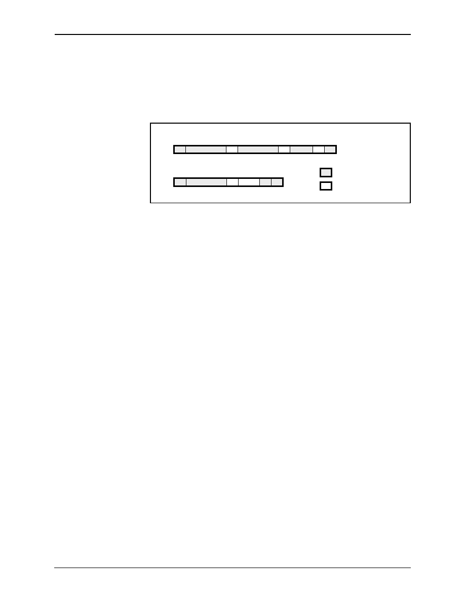
Figure 3-15. I2C Typical Protocol Diagram
DATAWRITE
DATAREAD
S
CHIP ADDR
A
SUB-ADDR
8 BITS
A
DATA
A
P
S
P
A
NA
= START
= STOP
= ACKNOWLEDGE
= NON ACKNOWLEDGE
S
CHIP ADDR
A
DATA NA
P
From Bt8xx to Slave
From Slave to Bt8xx
879A_046
相关PDF资料 |
PDF描述 |
|---|---|
| FVXO-HC53BR-FREQ | VCXO, CLOCK, 0.75 MHz - 250 MHz, HCMOS OUTPUT |
| FVXO-HC72BR-FREQ | VCXO, CLOCK, 0.75 MHz - 180 MHz, HCMOS OUTPUT |
| FVXO-HC73B-FREQ | VCXO, CLOCK, 0.75 MHz - 250 MHz, HCMOS OUTPUT |
| FVXO-LC52BR-FREQ | VCXO, CLOCK, 0.75 MHz - 1000 MHz, LVDS OUTPUT |
| FVXO-LC72BR-FREQ | VCXO, CLOCK, 0.75 MHz - 1000 MHz, LVDS OUTPUT |
相关代理商/技术参数 |
参数描述 |
|---|---|
| FUSZ03 | 制造商:Honeywell Sensing and Control 功能描述: |
| FUTURE 1AA PLUS | 制造商:Ansmann 功能描述: 制造商:ANSMANN AG 功能描述: |
| FUTURE 2AA PLUS | 制造商:Ansmann 功能描述: 制造商:ANSMANN AG 功能描述: |
| FUTURE 2C PLUS | 制造商:Ansmann 功能描述: 制造商:ANSMANN AG 功能描述: |
| FUTURE 3D PLUS | 制造商:Ansmann 功能描述: 制造商:ANSMANN AG 功能描述: |
发布紧急采购,3分钟左右您将得到回复。