- 您现在的位置:买卖IC网 > PDF目录67592 > FUSION878A (CONEXANT SYSTEMS) COLOR SIGNAL DECODER, PQFP128 PDF资料下载
参数资料
| 型号: | FUSION878A |
| 厂商: | CONEXANT SYSTEMS |
| 元件分类: | 颜色信号转换 |
| 英文描述: | COLOR SIGNAL DECODER, PQFP128 |
| 封装: | PLASTIC, QFP-128 |
| 文件页数: | 96/180页 |
| 文件大小: | 2067K |
| 代理商: | FUSION878A |
第1页第2页第3页第4页第5页第6页第7页第8页第9页第10页第11页第12页第13页第14页第15页第16页第17页第18页第19页第20页第21页第22页第23页第24页第25页第26页第27页第28页第29页第30页第31页第32页第33页第34页第35页第36页第37页第38页第39页第40页第41页第42页第43页第44页第45页第46页第47页第48页第49页第50页第51页第52页第53页第54页第55页第56页第57页第58页第59页第60页第61页第62页第63页第64页第65页第66页第67页第68页第69页第70页第71页第72页第73页第74页第75页第76页第77页第78页第79页第80页第81页第82页第83页第84页第85页第86页第87页第88页第89页第90页第91页第92页第93页第94页第95页当前第96页第97页第98页第99页第100页第101页第102页第103页第104页第105页第106页第107页第108页第109页第110页第111页第112页第113页第114页第115页第116页第117页第118页第119页第120页第121页第122页第123页第124页第125页第126页第127页第128页第129页第130页第131页第132页第133页第134页第135页第136页第137页第138页第139页第140页第141页第142页第143页第144页第145页第146页第147页第148页第149页第150页第151页第152页第153页第154页第155页第156页第157页第158页第159页第160页第161页第162页第163页第164页第165页第166页第167页第168页第169页第170页第171页第172页第173页第174页第175页第176页第177页第178页第179页第180页
1.0 Product Overview
Fusion 878A
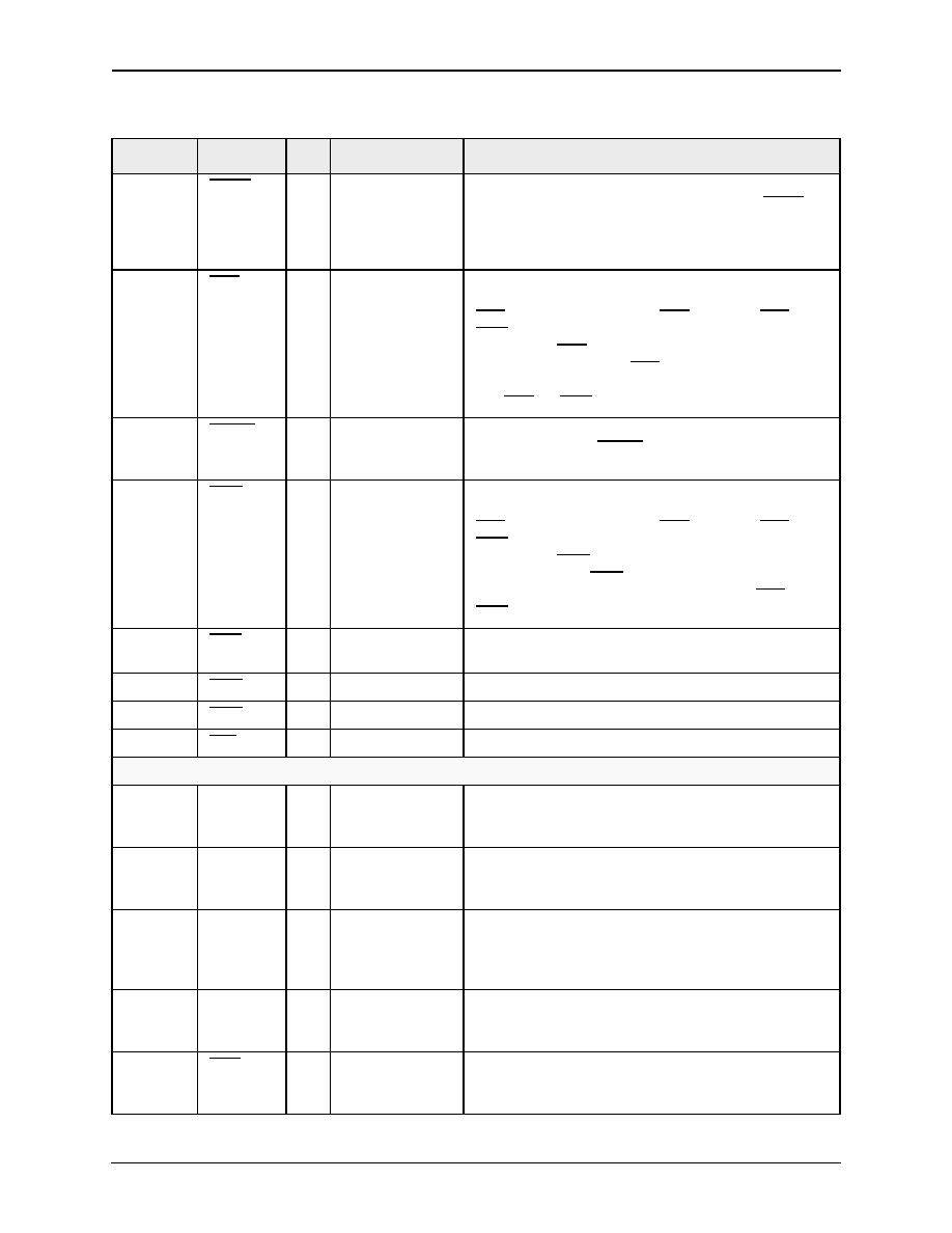
1.3 Pin Descriptions
PCI Video Decoder
1-10
Conexant
100600B
25
FRAME
I/O
Cycle Frame
This sustained, three-state signal is driven by the current master
to indicate the beginning and duration of an access. FRAME is
asserted to signal the beginning of a bus transaction. Data
transfer continues throughout assertion. At de-assertion, the
transaction is in the final data phase.
26
IRDY
I/O
Initiator Ready
This sustained, three-state signal indicates the bus master’s
readiness to complete the current data phase.
IRDY is used in conjunction with TRDY. When both IRDY and
TRDY are asserted, a data phase is completed on that clock.
During a read, IRDY indicates when the initiator is ready to
accept data. During a write, IRDY indicates when the initiator
has placed valid data on AD[31:0]. Wait cycles are inserted until
both IRDY and TRDY are asserted together.
28
DEVSEL
I/O
Device Select
This sustained, three-state signal indicates device selection.
When actively driven, DEVSEL indicates the driving device has
decoded its address as the target of the current access.
27
TRDY
I/O
Target Ready
This sustained, three-state signal indicates the target’s
readiness to complete the current data phase.
IRDY is used in conjunction with TRDY. When both IRDY and
TRDY are asserted, a data phase is completed on that clock.
During a read, TRDY indicates when the target is presenting
data. During a write, TRDY indicates when the target is ready to
accept the data. Wait cycles are inserted until both IRDY and
TRDY are asserted together.
29
STOP
I/O
Stop
This sustained, three-state signal indicates the target is
requesting the master to stop the current transaction.
30
PERR
I/O
Parity Error
Report data parity error.
31
SERR
O
System Error
Report address parity error. Open drain.
126
INTA
O
Interrupt A
This signal is an open drain interrupt output.
JTAG (5 Pins)
122
TCK
I
Test Clock
Used to synchronize all JTAG test structures. When JTAG
operations are not being performed, this pin must be driven to a
logical low.
123
TMS
I
Test Mode Select
JTAG input pin whose transitions drive the JTAG state machine
through its sequences. When JTAG operations are not being
performed, this pin must be left floating or tied high.
125
TDI
I
Test Data Input
JTAG pin used for loading instructions to the TAP controller or
for loading test vector data for boundary-scan operation. When
JTAG operations are not being performed, this pin must be left
floating or tied high.
124
TDO
O
Test Data Output
JTAG pin used for verifying test results of all JTAG sampling
operations. This output pin is active for certain JTAG operations
and will be three-stated at all other times.
121
TRST
I
Test Reset
JTAG pin used to initialize the JTAG controller. When JTAG
operations are not being performed, this pin must be driven to a
logical low.
Table 1-2. Pin Descriptions Grouped by Pin Function (2 of 4)
Pin #
Pin Name
I/O
Signal
Description
相关PDF资料 |
PDF描述 |
|---|---|
| FVXO-HC53BR-FREQ | VCXO, CLOCK, 0.75 MHz - 250 MHz, HCMOS OUTPUT |
| FVXO-HC72BR-FREQ | VCXO, CLOCK, 0.75 MHz - 180 MHz, HCMOS OUTPUT |
| FVXO-HC73B-FREQ | VCXO, CLOCK, 0.75 MHz - 250 MHz, HCMOS OUTPUT |
| FVXO-LC52BR-FREQ | VCXO, CLOCK, 0.75 MHz - 1000 MHz, LVDS OUTPUT |
| FVXO-LC72BR-FREQ | VCXO, CLOCK, 0.75 MHz - 1000 MHz, LVDS OUTPUT |
相关代理商/技术参数 |
参数描述 |
|---|---|
| FUSZ03 | 制造商:Honeywell Sensing and Control 功能描述: |
| FUTURE 1AA PLUS | 制造商:Ansmann 功能描述: 制造商:ANSMANN AG 功能描述: |
| FUTURE 2AA PLUS | 制造商:Ansmann 功能描述: 制造商:ANSMANN AG 功能描述: |
| FUTURE 2C PLUS | 制造商:Ansmann 功能描述: 制造商:ANSMANN AG 功能描述: |
| FUTURE 3D PLUS | 制造商:Ansmann 功能描述: 制造商:ANSMANN AG 功能描述: |
发布紧急采购,3分钟左右您将得到回复。