- 您现在的位置:买卖IC网 > Datasheet目录327 > HW-V5-ML561-UNI-G (Xilinx Inc)EVALUATION PLATFORM VIRTEX-5 Datasheet资料下载
参数资料
| 型号: | HW-V5-ML561-UNI-G |
| 厂商: | Xilinx Inc |
| 文件页数: | 36/140页 |
| 文件大小: | 0K |
| 描述: | EVALUATION PLATFORM VIRTEX-5 |
| 产品变化通告: | Adapter Replacement 23/May/2008 Development Systems Discontinuation 16/Jan/2012 |
| 标准包装: | 1 |
| 系列: | Virtex®-5 LXT |
| 类型: | FPGA |
| 适用于相关产品: | XC5VLX50T-FFG1136 |
| 所含物品: | 开发平台,小型闪存卡,缆线,DDR2 DIMM,电源和软件 |
| 相关产品: | XC5VLX50T-3FFG665C-ND - IC FPGA VIRTEX-5 50K 665FCBGA XC5VLX50T-3FFG1136C-ND - IC FPGA VIRTEX-5 50K 1136FBGA XC5VLX50T-3FF665C-ND - IC FPGA VIRTEX-5 50K 665FCBGA XC5VLX50T-3FF1136C-ND - IC FPGA VIRTEX-5 50K 1136FBGA XC5VLX50T-2FFG665I-ND - IC FPGA VIRTEX-5 50K 665FCBGA XC5VLX50T-2FFG665C-ND - IC FPGA VIRTEX-5 50K 665FCBGA XC5VLX50T-2FFG1136I-ND - IC FPGA VIRTEX-5 50K 1136FBGA XC5VLX50T-2FFG1136C-ND - IC FPGA VIRTEX-5 50K 1136FBGA XC5VLX50T-2FF665I-ND - IC FPGA VIRTEX-5 50K 665FCBGA XC5VLX50T-2FF665C-ND - IC FPGA VIRTEX-5 50K 665FCBGA 更多... |
第1页第2页第3页第4页第5页第6页第7页第8页第9页第10页第11页第12页第13页第14页第15页第16页第17页第18页第19页第20页第21页第22页第23页第24页第25页第26页第27页第28页第29页第30页第31页第32页第33页第34页第35页当前第36页第37页第38页第39页第40页第41页第42页第43页第44页第45页第46页第47页第48页第49页第50页第51页第52页第53页第54页第55页第56页第57页第58页第59页第60页第61页第62页第63页第64页第65页第66页第67页第68页第69页第70页第71页第72页第73页第74页第75页第76页第77页第78页第79页第80页第81页第82页第83页第84页第85页第86页第87页第88页第89页第90页第91页第92页第93页第94页第95页第96页第97页第98页第99页第100页第101页第102页第103页第104页第105页第106页第107页第108页第109页第110页第111页第112页第113页第114页第115页第116页第117页第118页第119页第120页第121页第122页第123页第124页第125页第126页第127页第128页第129页第130页第131页第132页第133页第134页第135页第136页第137页第138页第139页第140页
�� �
�
�Chapter� 3:� Hardware� Description�
��R�
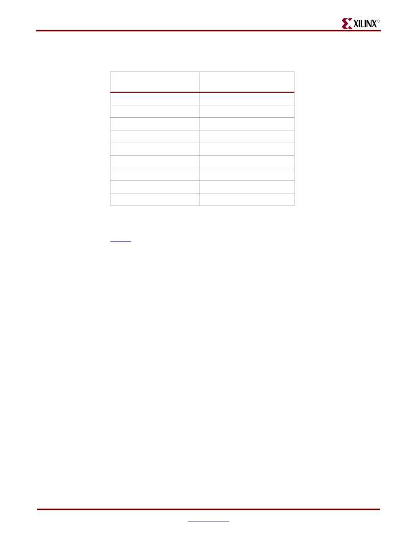
�Table� 3-18:�
�Headers� for� Voltage� Regulator� Inhibition�
�Power� Regulator�
�V� CCINT� (VR6)�
�SSTL18� (VR1)�
�SSTL18_M� (VR4)�
�SSTL2� (VR9)�
�SSTL2_M� (VR2)�
�HSTL� (VR10)�
�HSTL_M� (VR14)�
�V� CCAUX� (VR12)�
�VCC3V3� (VR13)�
�Inhibit� Header�
�P63�
�P11�
�P32�
�P68�
�P5�
�P74�
�P105�
�P79�
�P101�
�Board� Design� Considerations�
��and� guidelines� to� be� followed� for� designing� a� board� for� a� MIG� reference� design.�
�The� Virtex-5� FPGA� ML561� Development� Board� design� allows� implementation� of� DCI�
�termination� scheme� at� the� FPGA� for� each� of� the� memory� interfaces� on� the� board.� A�
�preliminary� analysis� of� the� Weighted� Average� Simultaneously� Switching� Outputs�
�(WASSO)� for� all� three� Virtex-5� devices� indicates� that� the� SSO� guidelines� are� met� for� the�
�current� pinout.� The� following� factors� helped� to� reduce� the� SSO� noise� as� compared� to� the�
�Virtex-4� FPGA� ML461� board� implementation:�
�?�
�?�
�?�
�SparseChevron� pinout� resulting� in� larger� number� of� Power/GND� pin� pairs� per� bank�
�A� revised� higher� SSO� allowance� per� Power/GND� pair� for� SparseChevron� packages�
�Reduced� thickness� of� the� board� (74� mils� vs.� 98� mils)� resulting� in� reduced� via�
�inductance�
�External� terminations� at� both� the� memory� and� FPGA� are� provided� for� data� signals� for�
�most� of� the� memory� interfaces� on� the� Virtex-5� FPGA� ML561� Development� Board� layout.�
�The� external� V� TT� termination� is� implemented� with� a� single� 50� Ω� termination� to� the� V� REF�
�level.� See� Chapter� 5,� “Signal� Integrity� Recommendations,”� for� specific� recommendations�
�and� guidelines� for� terminations.�
�These� are� V� TT� end� terminations� to� the� respective� voltage� levels� for� SSTL2,� SSTL18,� and�
�HSTL� signals.� There� are� two� topologies� of� end� terminations� for� data� signals:�
�1.�
�2.�
�Fly-by� termination:� The� parallel� termination� is� placed� after� the� receiver� pin.�
�Non-fly-by� termination:� The� parallel� termination� is� placed� between� the� driver� and� the�
�receiver� along� the� trace� as� close� to� the� receiver� pin� as� possible.� Also� the� stub� from�
�signal� trace� to� the� termination� resistor� is� kept� very� short,� within� 0.1� inch.�
�For� Read� data,� terminations� at� the� FPGA� have� non-fly-by� termination� topology.� These�
�terminations� can� be� selectively� depopulated� on� the� ML561� board� when� DCI� termination� is�
�implemented� inside� FPGA� for� received� data.� Due� to� non-fly-by� termination� topology,� the�
�result� is� a� minimal� stub� for� the� signal,� thus� preserving� good� signal� integrity� for� read� data.�
�36�
��Virtex-5� FPGA� ML561� User� Guide�
�UG199� (v1.2.1)� June� 15,� 2009�
�相关PDF资料 |
PDF描述 |
|---|---|
| I-JET | JTAG ARM DEBUGGING PROBE |
| IAC24A | INPUT MODULE AC 5MA 24VDC |
| IAC5EQ | INPUT MODULE AC 10MA 5VDC |
| IB8RM | SURGE SUPP 8OUT 12'CORD W/REMOTE |
| IBAR12-20T | SURGE SUPPRSSR 20A 12OUT RACKMNT |
相关代理商/技术参数 |
参数描述 |
|---|---|
| HW-V5-ML561-UNI-G-J | 功能描述:EVALUATION PLATFORM VIRTEX-5 RoHS:是 类别:编程器,开发系统 >> 通用嵌入式开发板和套件(MCU、DSP、FPGA、CPLD等) 系列:Virtex®-5 LXT 产品培训模块:Blackfin® Processor Core Architecture Overview Blackfin® Device Drivers Blackfin® Optimizations for Performance and Power Consumption Blackfin® System Services 特色产品:Blackfin? BF50x Series Processors 标准包装:1 系列:Blackfin® 类型:DSP 适用于相关产品:ADSP-BF548 所含物品:板,软件,4x4 键盘,光学拨轮,QVGA 触摸屏 LCD 和 40G 硬盘 配用:ADZS-BFBLUET-EZEXT-ND - EZ-EXTENDER DAUGHTERBOARDADZS-BFLLCD-EZEXT-ND - BOARD EXT LANDSCAP LCD INTERFACE 相关产品:ADSP-BF542BBCZ-4A-ND - IC DSP 16BIT 400MHZ 400CSBGAADSP-BF544MBBCZ-5M-ND - IC DSP 16BIT 533MHZ MDDR 400CBGAADSP-BF542MBBCZ-5M-ND - IC DSP 16BIT 533MHZ MDDR 400CBGAADSP-BF542KBCZ-6A-ND - IC DSP 16BIT 600MHZ 400CSBGAADSP-BF547MBBCZ-5M-ND - IC DSP 16BIT 533MHZ MDDR 400CBGAADSP-BF548BBCZ-5A-ND - IC DSP 16BIT 533MHZ 400CSBGAADSP-BF547BBCZ-5A-ND - IC DSP 16BIT 533MHZ 400CSBGAADSP-BF544BBCZ-5A-ND - IC DSP 16BIT 533MHZ 400CSBGAADSP-BF542BBCZ-5A-ND - IC DSP 16BIT 533MHZ 400CSBGA |
| HW-V5-PCIE2-UNI-G | 功能描述:KIT DEV PCIEXPRESS GTX VIRTEX5 RoHS:是 类别:编程器,开发系统 >> 通用嵌入式开发板和套件(MCU、DSP、FPGA、CPLD等) 系列:Virtex® -5 产品培训模块:Blackfin® Processor Core Architecture Overview Blackfin® Device Drivers Blackfin® Optimizations for Performance and Power Consumption Blackfin® System Services 特色产品:Blackfin? BF50x Series Processors 标准包装:1 系列:Blackfin® 类型:DSP 适用于相关产品:ADSP-BF548 所含物品:板,软件,4x4 键盘,光学拨轮,QVGA 触摸屏 LCD 和 40G 硬盘 配用:ADZS-BFBLUET-EZEXT-ND - EZ-EXTENDER DAUGHTERBOARDADZS-BFLLCD-EZEXT-ND - BOARD EXT LANDSCAP LCD INTERFACE 相关产品:ADSP-BF542BBCZ-4A-ND - IC DSP 16BIT 400MHZ 400CSBGAADSP-BF544MBBCZ-5M-ND - IC DSP 16BIT 533MHZ MDDR 400CBGAADSP-BF542MBBCZ-5M-ND - IC DSP 16BIT 533MHZ MDDR 400CBGAADSP-BF542KBCZ-6A-ND - IC DSP 16BIT 600MHZ 400CSBGAADSP-BF547MBBCZ-5M-ND - IC DSP 16BIT 533MHZ MDDR 400CBGAADSP-BF548BBCZ-5A-ND - IC DSP 16BIT 533MHZ 400CSBGAADSP-BF547BBCZ-5A-ND - IC DSP 16BIT 533MHZ 400CSBGAADSP-BF544BBCZ-5A-ND - IC DSP 16BIT 533MHZ 400CSBGAADSP-BF542BBCZ-5A-ND - IC DSP 16BIT 533MHZ 400CSBGA |
| HW-VID-KIT | 功能描述:可编程逻辑 IC 开发工具 Lattice Video Interface Kit RoHS:否 制造商:Altera Corporation 产品:Development Kits 类型:FPGA 工具用于评估:5CEFA7F3 接口类型: 工作电源电压: |
| HW-VL1 | 制造商:IDEC CORPORATION 功能描述:BARRIER |
| HW-VL2 | 制造商:IDEC Corporation 功能描述:COVER;HW FNGR SAFE CONTAC CVR 制造商:IDEC CORPORATION 功能描述:HW FNGR SAFE CONTAC CVR |
发布紧急采购,3分钟左右您将得到回复。