参数资料
| 型号: | HW-XGI-VIDEO-US |
| 厂商: | Xilinx Inc |
| 文件页数: | 37/68页 |
| 文件大小: | 0K |
| 描述: | DAUGHTER CARD VIDEO I/O VIODC |
| 标准包装: | 1 |
| 其它名称: | 122-1506 HW-XGI-VIDEO-US-ND |
第1页第2页第3页第4页第5页第6页第7页第8页第9页第10页第11页第12页第13页第14页第15页第16页第17页第18页第19页第20页第21页第22页第23页第24页第25页第26页第27页第28页第29页第30页第31页第32页第33页第34页第35页第36页当前第37页第38页第39页第40页第41页第42页第43页第44页第45页第46页第47页第48页第49页第50页第51页第52页第53页第54页第55页第56页第57页第58页第59页第60页第61页第62页第63页第64页第65页第66页第67页第68页
�� �
�
�R�
�Bus� Interface�
�(black� arrows).� It� is� also� important� to� note� that� the� VCO� frequency� range� and� charge� pump�
�currents� must� be� configured� to� match� the� expected� frequency.�
�Sample�
�RGB�
�10�
�11�
�0�
�1�
�2�
�3�
�4�
�5�
�6�
�7�
�8�
�9�
�10�
�11�
�0�
�HSYNC�
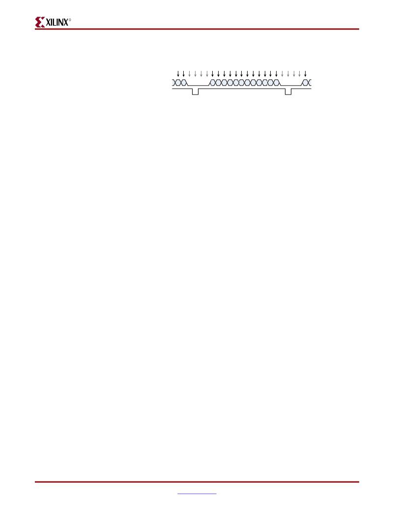
�Figure� 4-5:� Ideal� ADC� Sampling� Positions�
�Setting� the� feedback� divider� correctly� results� in� the� correct� sample� frequency,� but� the�
�sample� phase� must� also� be� set.� Under� ideal� conditions,� the� phase� delay� would� be� T/2,� to�
�sample� at� the� center� of� the� pixels.� This� makes� T/2� a� reasonable� default� value.� Under� actual�
�operating� conditions,� there� can� be� skew� between� the� HSYNC� signal� and� the� video� data�
�thus� requiring� phase� adjustment.�
�The� process� above� is� quite� straightforward� if� one� knows� the� proper� settings� for� a� given�
�source.� VESA� timing� standards� are� a� good� place� to� start� for� standard� resolutions.�
�Unfortunately,� graphics� adapters� often� do� not� follow� these� exactly.� In� this� case,� the� PLL�
�divider� value� and� phase� must� be� adjusted� to� properly� digitize� the� source.� This� process� is�
�beyond� the� scope� of� this� document.�
�Setting� Black� Levels�
�The� primary� mechanism� for� setting� the� black� level� is� the� input� clamp.� This� clamps� the�
�input� to� ground,� resulting� in� a� DC� offset� in� the� coupling� capacitor� (just� outside� the�
�AD9887A)� equal� to� the� difference� between� the� current� input� voltage� and� ground.� After� the�
�clamp� is� released,� this� difference� is� effectively� subtracted� from� the� raw� input� signal,�
�resulting� in� an� input� signal� reference� to� ground.� For� this� circuit� to� function� properly,� this�
�clamp� should� only� be� enabled� when� the� input� data� is� known� to� be� black,� such� as� during� the�
�horizontal� back� porch.� The� AD9887A� has� a� clamp� placement� register� to� control� the� start� of�
�the� clamp,� in� cycles� after� the� falling� edge� of� HSYNC.� The� clamp� duration� register� controls�
�the� length� of� the� clamp,� in� cycles.�
�The� AD9887A� also� includes� offset� registers� to� offset� the� black� level� of� each� color�
�individually.� This� control� is� typically� not� needed.�
�Setting� Gain�
�The� AD9887A� includes� gain� registers� to� adjust� the� input� range� of� the� ADC.� Setting� this� too�
�low� results� in� a� dim� display,� while� setting� it� too� high� results� in� saturation� and� clipping� of�
�brighter� colors.�
�Bus� Interface�
�The� AD9887A� data� output� is� synchronous� to� a� differential� clock,� DATACK.� The� pixel� data�
�is� 8� bits� per� color.� There� are� two� pixel� buses,� A� and� B.� There� are� also� three� key� sync� signals�
�–� HS,� VS,� and� DE.�
�The� data� bus� can� be� operated� in� either� single� pixel� mode� or� dual� pixel� mode.� Single� pixel�
�mode� only� uses� port� A� and� the� clock� rate� is� equal� to� the� pixel� rate.� In� dual� pixel� mode,� port�
�A� carries� even� pixels� and� port� B� carries� odd� pixels,� and� the� clock� rate� is� half� the� pixel� rate.�
�The� single� pixel� more� would� be� desirable� to� reduce� the� number� of� signals,� but� the�
�AD9887A� has� a� max� DATACK� frequency� of� 140� MHz,� so� for� pixel� rates� greater� than�
�140� MHz,� the� bus� has� to� be� operated� in� dual� pixel� mode.�
�Video� Input/Output� Daughter� Card�
�UG235� (v1.2.1)� October� 31,� 2007�
��37�
�相关PDF资料 |
PDF描述 |
|---|---|
| ICD15S13E6GV00LF | CONN DSUB HD SOCKT 15POS R/A PCB |
| ICD26S13E4GX00LF | CONN DSUB HD SOCKT 26POS R/A PCB |
| ID09S33E4GV00LF | CONN RCPT 9POS R/A GOLD |
| ID451000 | CONN RECPT USB A ADAPTER |
| IELHK11-1-72-70.0-01-V | CIRCUIT BREAKER HYMAG DP 70A |
相关代理商/技术参数 |
参数描述 |
|---|---|
| HWXX35338TR | 制造商:Vishay Intertechnologies 功能描述: |
| HWXX38438 | 制造商:Vishay Semiconductors 功能描述: |
| HWZ1408 | 制造商:OHIO BUCKEYE 功能描述: |
| HWZ1424 | 制造商:OHIO BUCKEYE 功能描述: |
| HWZ1620 | 制造商:OHIO BUCKEYE 功能描述: |
发布紧急采购,3分钟左右您将得到回复。