- 您现在的位置:买卖IC网 > PDF目录10966 > MCR705JP7CDWE (Freescale Semiconductor)MCU 8BIT 224B RAM 28-SOIC PDF资料下载
参数资料
| 型号: | MCR705JP7CDWE |
| 厂商: | Freescale Semiconductor |
| 文件页数: | 161/164页 |
| 文件大小: | 0K |
| 描述: | MCU 8BIT 224B RAM 28-SOIC |
| 标准包装: | 26 |
| 系列: | HC05 |
| 核心处理器: | HC05 |
| 芯体尺寸: | 8-位 |
| 速度: | 2.1MHz |
| 连通性: | SIO |
| 外围设备: | POR,温度传感器,WDT |
| 输入/输出数: | 22 |
| 程序存储器容量: | 6KB(6K x 8) |
| 程序存储器类型: | OTP |
| RAM 容量: | 224 x 8 |
| 电压 - 电源 (Vcc/Vdd): | 2.7 V ~ 5.5 V |
| 数据转换器: | A/D 4x12b |
| 振荡器型: | 内部 |
| 工作温度: | -40°C ~ 85°C |
| 封装/外壳: | 28-SOIC(0.295",7.50mm 宽) |
| 包装: | 管件 |
第1页第2页第3页第4页第5页第6页第7页第8页第9页第10页第11页第12页第13页第14页第15页第16页第17页第18页第19页第20页第21页第22页第23页第24页第25页第26页第27页第28页第29页第30页第31页第32页第33页第34页第35页第36页第37页第38页第39页第40页第41页第42页第43页第44页第45页第46页第47页第48页第49页第50页第51页第52页第53页第54页第55页第56页第57页第58页第59页第60页第61页第62页第63页第64页第65页第66页第67页第68页第69页第70页第71页第72页第73页第74页第75页第76页第77页第78页第79页第80页第81页第82页第83页第84页第85页第86页第87页第88页第89页第90页第91页第92页第93页第94页第95页第96页第97页第98页第99页第100页第101页第102页第103页第104页第105页第106页第107页第108页第109页第110页第111页第112页第113页第114页第115页第116页第117页第118页第119页第120页第121页第122页第123页第124页第125页第126页第127页第128页第129页第130页第131页第132页第133页第134页第135页第136页第137页第138页第139页第140页第141页第142页第143页第144页第145页第146页第147页第148页第149页第150页第151页第152页第153页第154页第155页第156页第157页第158页第159页第160页当前第161页第162页第163页第164页
Simple Synchronous Serial Interface
MC68HC705JJ7 MC68HC705JP7 Advance Information Data Sheet, Rev. 4.1
96
Freescale Semiconductor
The SIOP subsystem shares its input/output pins with port B. When the SIOP is enabled (SPE bit set in
the SCR), the port B data direction and data registers are bypassed by the SIOP. The port B data direction
and data registers will remain accessible and can be altered by the application software, but these actions
will not affect the SIOP transmitted or received data.
9.2 SIOP Signal Format
The SIOP subsystem can be software configured for master or slave operation. No external mode
selection inputs are available (for instance, no slave select pin).
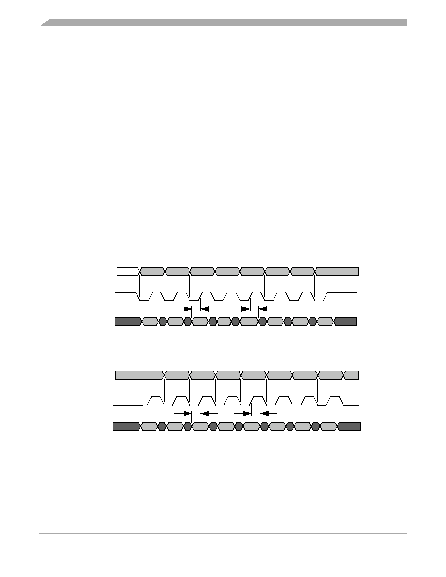
9.2.1 Serial Clock (SCK)
The state of the SCK output remains a fixed logic level during idle periods between data transfers. The
edges of SCK indicate the beginning of each output data transfer and latch any incoming data received.
The first bit of transmitted data is output from the SDO pin on the first falling edge of SCK. The first bit of
received data is accepted at the SDI pin on the first rising edge of SCK after the first falling edge. The
transfer is terminated upon the eighth rising edge of SCK.
The idle state of the SCK is determined by the state of the CPHA bit in the SCR. When the CPHA is clear,
SCK will remain idle at a logic 1 as shown in Figure 9-2. When the CPHA is set, SCK will remain idle at
a logic 0 as shown in Figure 9-3. In both cases, the SDO changes data on the falling edge of the SCK,
and the SDI latches data in on the rising edge of SCK.
Figure 9-2. SIOP Timing Diagram (CPHA = 0)
Figure 9-3. SIOP Timing Diagram (CPHA = 1)
The only difference in the master and slave modes of operation is the sourcing of the SCK. In master
mode, SCK is driven from an internal source within the MCU. In slave mode, SCK is driven from a source
external to the MCU. The SCK frequency is based on one of four divisions of the oscillator clock that is
selected by the SPR0 and SPR1 bits in the SCR.
SCK
SDO
SDI
100 ns
BIT 1
BIT 2
BIT 3
BIT 4
BIT 5
BIT 6
BIT 7
BIT 8
BIT 1
BIT 2
BIT 3
BIT 4
BIT 5
BIT 6
BIT 7
BIT 8
(CPHA = 0)
(IDLE = 1)
SCK
SDO
SDI
100 ns
BIT 1
BIT 2
BIT 3
BIT 4
BIT 5
BIT 6
BIT 7
BIT 8
BIT 1
BIT 2
BIT 3
BIT 4
BIT 5
BIT 6
BIT 7
BIT 8
(CPHA = 1)
(IDLE = 0)
相关PDF资料 |
PDF描述 |
|---|---|
| MCHC705JP7CDWE | IC MCU 8BIT 224 BYTES RAM 28SOIC |
| LF13WBJ-20P | CONN JACK WATERPROOF 20POS MALE |
| MK20DX128VMP5 | IC ARM CORTEX MCU 128KB 64BGA |
| MC908AP8ACBE | IC MCU 8K FLASH 8MHZ 42-SDIP |
| VE-2N2-IY-F2 | CONVERTER MOD DC/DC 15V 50W |
相关代理商/技术参数 |
参数描述 |
|---|---|
| MCR706A | 制造商:MOTOROLA 制造商全称:Motorola, Inc 功能描述:Silicon Controlled Rectifiers |
| MCR706AT4 | 功能描述:SCR 400V 4A RoHS:否 制造商:STMicroelectronics 最大转折电流 IBO:480 A 额定重复关闭状态电压 VDRM:600 V 关闭状态漏泄电流(在 VDRM IDRM 下):5 uA 开启状态 RMS 电流 (It RMS): 正向电压下降:1.6 V 栅触发电压 (Vgt):1.3 V 最大栅极峰值反向电压:5 V 栅触发电流 (Igt):35 mA 保持电流(Ih 最大值):75 mA 安装风格:Through Hole 封装 / 箱体:TO-220 封装:Tube |
| MCR706AT4G | 功能描述:SCR THY 4A 400V SCR RoHS:否 制造商:STMicroelectronics 最大转折电流 IBO:480 A 额定重复关闭状态电压 VDRM:600 V 关闭状态漏泄电流(在 VDRM IDRM 下):5 uA 开启状态 RMS 电流 (It RMS): 正向电压下降:1.6 V 栅触发电压 (Vgt):1.3 V 最大栅极峰值反向电压:5 V 栅触发电流 (Igt):35 mA 保持电流(Ih 最大值):75 mA 安装风格:Through Hole 封装 / 箱体:TO-220 封装:Tube |
| MCR707A | 制造商:MOTOROLA 制造商全称:Motorola, Inc 功能描述:Silicon Controlled Rectifiers |
| MCR708A | 功能描述:SCR 600V 4A RoHS:否 制造商:STMicroelectronics 最大转折电流 IBO:480 A 额定重复关闭状态电压 VDRM:600 V 关闭状态漏泄电流(在 VDRM IDRM 下):5 uA 开启状态 RMS 电流 (It RMS): 正向电压下降:1.6 V 栅触发电压 (Vgt):1.3 V 最大栅极峰值反向电压:5 V 栅触发电流 (Igt):35 mA 保持电流(Ih 最大值):75 mA 安装风格:Through Hole 封装 / 箱体:TO-220 封装:Tube |
发布紧急采购,3分钟左右您将得到回复。