- 您现在的位置:买卖IC网 > PDF目录262949 > MT45W2MV16BAFB-706LIT 2M X 16 PSEUDO STATIC RAM, 70 ns, PBGA54 PDF资料下载
参数资料
| 型号: | MT45W2MV16BAFB-706LIT |
| 元件分类: | SRAM |
| 英文描述: | 2M X 16 PSEUDO STATIC RAM, 70 ns, PBGA54 |
| 封装: | FBGA-54 |
| 文件页数: | 52/55页 |
| 文件大小: | 816K |
| 代理商: | MT45W2MV16BAFB-706LIT |
第1页第2页第3页第4页第5页第6页第7页第8页第9页第10页第11页第12页第13页第14页第15页第16页第17页第18页第19页第20页第21页第22页第23页第24页第25页第26页第27页第28页第29页第30页第31页第32页第33页第34页第35页第36页第37页第38页第39页第40页第41页第42页第43页第44页第45页第46页第47页第48页第49页第50页第51页当前第52页第53页第54页第55页
2 MEG x 16
ASYNC/PAGE/BURST CellularRAM MEMORY
ADVANCE
09005aef80ec6f63
Micron Technology, Inc., reserves the right to change products or specifications without notice.
Burst CellularRAM_32.fm - Rev. A 2/18/04 EN
6
2004 Micron Technology, Inc. All Rights Reserved.
l
NOTE:
The CLK and ADV# inputs can be tied to VSS if the device is always operating in asynchronous or page mode. WAIT will
be asserted but should be ignored during asynchronous and page mode operations.
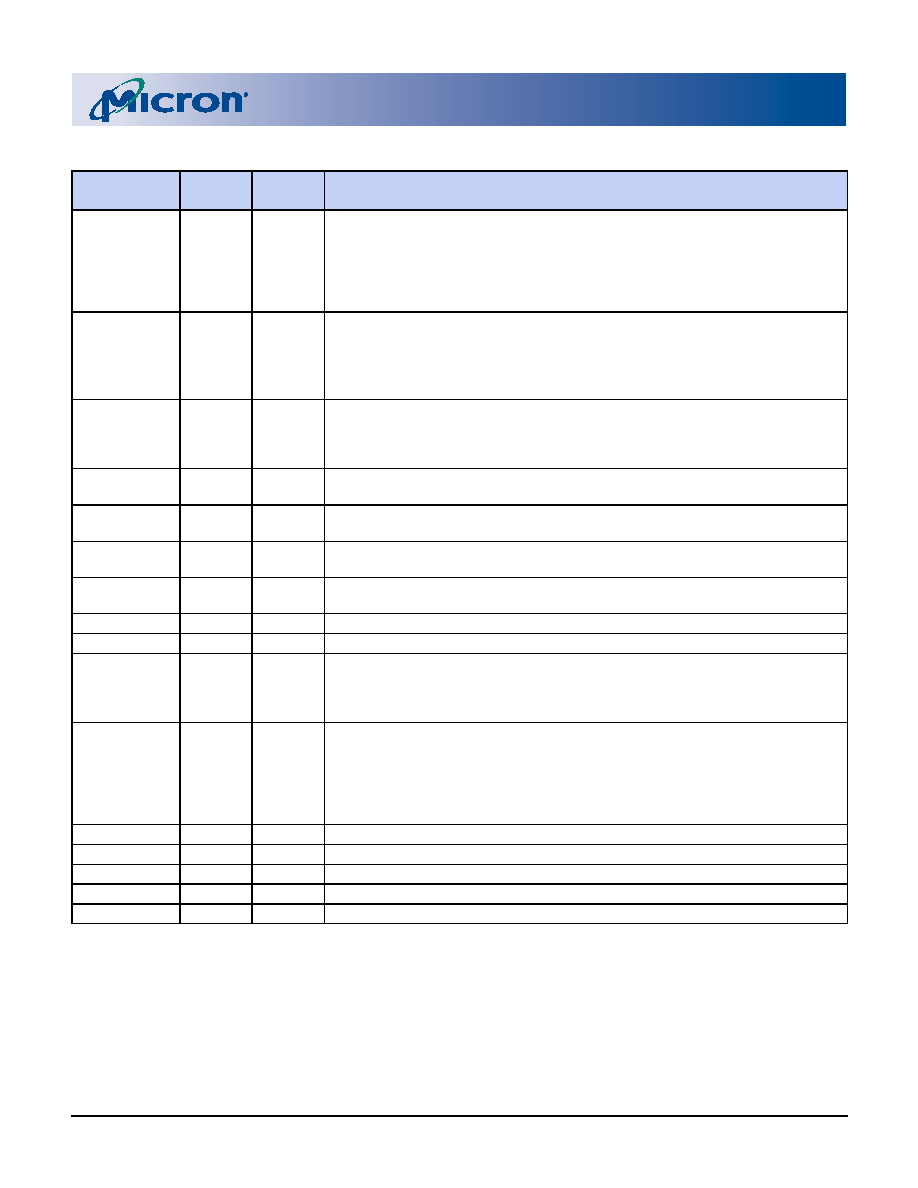
Table 1:
FBGA Ball Descriptions
FBGA
ASSIGNMENT
SYMBOL
TYPE
DESCRIPTION
A3, A4, A5, B3,
B4, C3, C4, D4,
H2, H3, H4, H5,
G3, G4, F3, F4,
E4, D3, H1, G2,
H6
A[20:0]
Input
Address Inputs: Inputs for addresses during READ and WRITE operations.
Addresses are internally latched during READ and WRITE cycles. The address lines
are also used to define the value to be loaded into the bus configuration register
or the refresh configuration register.
J2
CLK
Input
Clock: Synchronizes the memory to the system operating frequency during
synchronous operations. When configured for synchronous operation, the address
is latched on the first rising CLK edge when ADV# is active
. CLK is static (HIGH or
LOW) during asynchronous access READ and WRITE operations and during PAGE
READ ACCESS operations.
J3
ADV#
Input
Address Valid: Indicates that a valid address is present on the address inputs.
Addresses can be latched on the rising edge of ADV# during asynchronous READ
and WRITE operations. ADV# can be held LOW during asynchronous READ and
WRITE operations.
A6
CRE
Input
Configuration Register Enable: When CRE is HIGH, WRITE operations load the
refresh configuration register or bus configuration register.
B5
CE#
Input
Chip Enable: Activates the device when LOW. When CE# is HIGH, the device is
disabled and goes into standby or deep power-down mode.
A2
OE#
Input
Output Enable: Enables the output buffers when LOW. When OE# is HIGH, the
output buffers are disabled.
G5
WE#
Input
Write Enable: Determines if a given cycle is a WRITE cycle. If WE# is LOW, the cycle
is a WRITE to either a configuration register or to the memory array.
A1
LB#
Input
Lower Byte Enable. DQ[7:0]
B2
UB#
Input
Upper Byte Enable. DQ[15:8]
B6, C5, C6, D5,
E5, F5, F6, G6,
B1, C1, C2, D2,
E2, F2, F1, G1
DQ[15:0]
Input/
Output
Data Inputs/Outputs.
J1
WAIT
Output
Wait: Provides data-valid feedback during burst READ and WRITE operations. The
signal is gated by CE#. WAIT is used to arbitrate collisions between refresh and
READ/WRITE operations. WAIT is asserted when a burst crosses a row boundary.
WAIT is also used to mask the delay associated with opening a new internal page.
WAIT is asserted and should be ignored during asynchronous and page mode
operations. WAIT is High-Z when CE# is HIGH.
E3, J4, J5, J6
NC
–
Not internally connected.
D6
VCC
Supply
Device Power Supply: (1.70V–1.95V) Power supply for device core operation.
E1
VCCQ
Supply
I/O Power Supply: (1.70V–1.95V) Power supply for input/output buffers.
E6
VSS
Supply
VSS must be connected to ground.
D1
VSSQ
Supply
VSSQ must be connected to ground.
相关PDF资料 |
PDF描述 |
|---|---|
| MT28C128532W30EBW-F705P856BTWT | SPECIALTY MEMORY CIRCUIT, PBGA77 |
| M93C66-MB6TP | 256 X 16 MICROWIRE BUS SERIAL EEPROM, DSO8 |
| MT48V8M16LFB4-75M:G | 8M X 16 SYNCHRONOUS DRAM, 5.4 ns, PBGA54 |
| MS8256FKXA-12 | 256K X 8 MULTI DEVICE SRAM MODULE, 120 ns, DMA32 |
| MT46V32M16BN-75IT | 32M X 16 DDR DRAM, 0.75 ns, PBGA60 |
相关代理商/技术参数 |
参数描述 |
|---|---|
| MT45W2MV16PFA-70 WT | 制造商:Micron Technology Inc 功能描述:2MX16 PSRAM PLASTIC WIRELESS TEMP FBGA 1.8V ASYNCH PSEUDO ST - Trays |
| MT45W2MW16BABB-706 L WT | 功能描述:IC PSRAM 32MBIT 70NS 54VFBGA RoHS:是 类别:集成电路 (IC) >> 存储器 系列:- 标准包装:378 系列:- 格式 - 存储器:闪存 存储器类型:FLASH 存储容量:8M(1M x 8,512K x 16) 速度:110ns 接口:并联 电源电压:2.7 V ~ 3.6 V 工作温度:-40°C ~ 85°C 封装/外壳:48-CBGA 供应商设备封装:48-CBGA(7x7) 包装:托盘 |
| MT45W2MW16BABB-706 L WT TR | 制造商:Micron Technology Inc 功能描述:PSRAM ASYNC 1 32MBIT 2MX16 70NS 54VFBGA - Tape and Reel |
| MT45W2MW16BABB-706 WT | 制造商:Micron Technology Inc 功能描述:PSRAM Async 1 32M-Bit 2M x 16 70ns 54-Pin VFBGA Tray 制造商:Micron Technology Inc 功能描述:PSRAM ASYNC 1 32MBIT 2MX16 70NS 54VFBGA - Trays 制造商:Micron Technology Inc 功能描述:IC PSRAM 32MBIT 70NS 54VFBGA |
| MT45W2MW16BABB-706 WT TR | 功能描述:IC PSRAM 32MBIT 70NS 54VFBGA RoHS:是 类别:集成电路 (IC) >> 存储器 系列:- 标准包装:96 系列:- 格式 - 存储器:闪存 存储器类型:FLASH 存储容量:16M(2M x 8,1M x 16) 速度:70ns 接口:并联 电源电压:2.65 V ~ 3.6 V 工作温度:-40°C ~ 85°C 封装/外壳:48-TFSOP(0.724",18.40mm 宽) 供应商设备封装:48-TSOP 包装:托盘 |
发布紧急采购,3分钟左右您将得到回复。