- 您现在的位置:买卖IC网 > PDF目录299581 > ORT82G5-2BM680 (LATTICE SEMICONDUCTOR CORP) FPGA, 1296 CLBS, 380000 GATES, PBGA680 PDF资料下载
参数资料
| 型号: | ORT82G5-2BM680 |
| 厂商: | LATTICE SEMICONDUCTOR CORP |
| 元件分类: | FPGA |
| 英文描述: | FPGA, 1296 CLBS, 380000 GATES, PBGA680 |
| 封装: | PLASTIC, BGA-680 |
| 文件页数: | 54/110页 |
| 文件大小: | 1459K |
| 代理商: | ORT82G5-2BM680 |
第1页第2页第3页第4页第5页第6页第7页第8页第9页第10页第11页第12页第13页第14页第15页第16页第17页第18页第19页第20页第21页第22页第23页第24页第25页第26页第27页第28页第29页第30页第31页第32页第33页第34页第35页第36页第37页第38页第39页第40页第41页第42页第43页第44页第45页第46页第47页第48页第49页第50页第51页第52页第53页当前第54页第55页第56页第57页第58页第59页第60页第61页第62页第63页第64页第65页第66页第67页第68页第69页第70页第71页第72页第73页第74页第75页第76页第77页第78页第79页第80页第81页第82页第83页第84页第85页第86页第87页第88页第89页第90页第91页第92页第93页第94页第95页第96页第97页第98页第99页第100页第101页第102页第103页第104页第105页第106页第107页第108页第109页第110页
48
Lattice Semiconductor
Data Sheet
January 25, 2002
8b/10b SERDES Backplane Interface FPSC
ORCA ORT82G5 1.0-1.25/2.0-2.5/3.125-3.5 Gbits/s
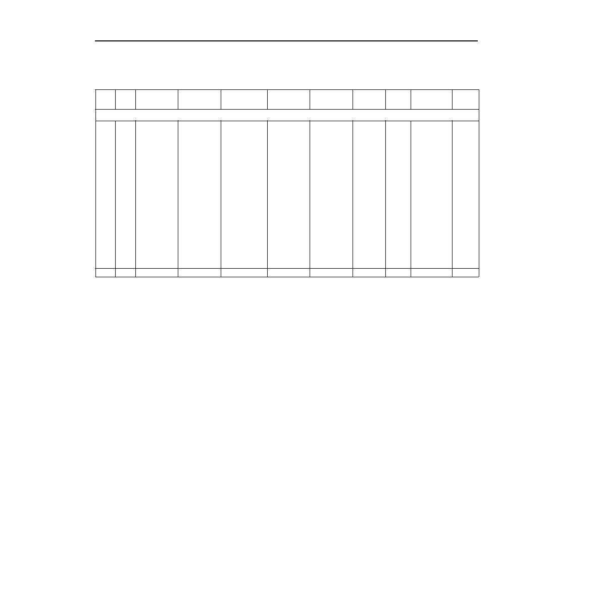
Memory Map (continued)
Table 18. Memory Map (continued)
Addr
(Hex)
Reg
#
DB0
DB1
DB2
DB3
DB4
DB5
DB6
DB7
Default
Value
SERDES A Global Control Register (Acts on Channels A, B, C, and D)
30005
—
GPRBS_A
Global Enable.
The GPRBS bit
globally enables
the PRBS gen-
erators and
checkers all
four channels of
SERDES A
when GPRBS =
1. GPRBS = 0
on device reset.
GMASK_A
Global Mask.
The GMASK
globally masks
all the channel
alarms of SER-
DES A when
GMASK = 1.
This prevents
all the transmit
and receive
alarms from
generating an
interrupt.
GMASK = 1 on
device reset.
GSWRST_A
RESET Func-
tion. The
GSWRST bit pro-
vides the same
function as the
hardware reset
for the transmit
and receive sec-
tions of all four
channels of
ASERDES A,
except that the
device congura-
tion settings are
not affected when
GSWRST is
asserted.
GSWRST = 0 on
device reset. This
is not a self-clear-
ing bit. Once set,
it must be cleared
by writing a 0 to it.
GPWRDNT_A
Powerdown
Transmit Func-
tion. When
GPWRDNT = 1,
sections of the
transmit hard-
ware for all four
channels of
SERDES A are
powered down
to conserve
power.
GPWRDNT = 0
on device reset.
GPWRDNR_A
Powerdown
Receive Func-
tion. When
GPWRDNR =
1, sections of
the receive
hardware for all
four channels of
SERDES A are
powered down
to conserve
power.
GPWRDNR = 0
on device reset.
GTRISTN_
A
Active-Low
TRISTN
Function.
When
GTRISTN =
0, the
CMOS out-
put buffers
for SER-
DES A are
3-stated.
GTRISTN =
1 on device
reset.
—
GTESTEN_A
Test Enable
Control. When
GTESTEN = 1,
the transmit
and receive
sections of all
four channels
of SERDES A
are placed in
test mode.
GTESTEN = 0
on device
reset.
44
30006
—
TestMode
—
RSVD
00
相关PDF资料 |
PDF描述 |
|---|---|
| ORT82G5-3BM680 | FPGA, 1296 CLBS, 380000 GATES, PBGA680 |
| OS10040280G-012 | FIBER OPTIC RECEIVER, 1290-1600nm, PANEL MOUNT, FC/APC CONNECTOR |
| OT-WBSC-Y-A-10-X-9-M-3-05-FA | FIBER OPTIC SPLITTER/COUPLER, 1X2PORT, 10.0, PANEL MOUNT, FC/APC CONNECTOR |
| OT-WBSC-Y-A-50-13-9-F-1-05-FA | FIBER OPTIC SPLITTER/COUPLER, 1X2PORT, 50.0, PANEL MOUNT, FC/APC CONNECTOR |
| OT-WBSC-Y-A-50-X-9-O-1-99-SA | FIBER OPTIC SPLITTER/COUPLER, 1X2PORT, 50.0, PANEL MOUNT, SC/APC CONNECTOR |
相关代理商/技术参数 |
参数描述 |
|---|---|
| ORT82G5-2BM680C | 功能描述:FPGA - 现场可编程门阵列 10368 LUT 372 I/O RoHS:否 制造商:Altera Corporation 系列:Cyclone V E 栅极数量: 逻辑块数量:943 内嵌式块RAM - EBR:1956 kbit 输入/输出端数量:128 最大工作频率:800 MHz 工作电源电压:1.1 V 最大工作温度:+ 70 C 安装风格:SMD/SMT 封装 / 箱体:FBGA-256 |
| ORT82G5-2BM680I | 功能描述:FPGA - 现场可编程门阵列 10368 LUT 372 I/O RoHS:否 制造商:Altera Corporation 系列:Cyclone V E 栅极数量: 逻辑块数量:943 内嵌式块RAM - EBR:1956 kbit 输入/输出端数量:128 最大工作频率:800 MHz 工作电源电压:1.1 V 最大工作温度:+ 70 C 安装风格:SMD/SMT 封装 / 箱体:FBGA-256 |
| ORT82G5-2F680C | 功能描述:FPGA - 现场可编程门阵列 ORCA FPSC 2.7Gbits/s BP XCVR 643K RoHS:否 制造商:Altera Corporation 系列:Cyclone V E 栅极数量: 逻辑块数量:943 内嵌式块RAM - EBR:1956 kbit 输入/输出端数量:128 最大工作频率:800 MHz 工作电源电压:1.1 V 最大工作温度:+ 70 C 安装风格:SMD/SMT 封装 / 箱体:FBGA-256 |
| ORT82G5-2F680I | 功能描述:FPGA - 现场可编程门阵列 ORCA FPSC 2.7GBITS/s BP XCVR 643K RoHS:否 制造商:Altera Corporation 系列:Cyclone V E 栅极数量: 逻辑块数量:943 内嵌式块RAM - EBR:1956 kbit 输入/输出端数量:128 最大工作频率:800 MHz 工作电源电压:1.1 V 最大工作温度:+ 70 C 安装风格:SMD/SMT 封装 / 箱体:FBGA-256 |
| ORT82G5-2FN680C | 功能描述:FPGA - 现场可编程门阵列 ORCA FPSC 1.5V 3.7 G b Bpln Xcvr 643K Gt RoHS:否 制造商:Altera Corporation 系列:Cyclone V E 栅极数量: 逻辑块数量:943 内嵌式块RAM - EBR:1956 kbit 输入/输出端数量:128 最大工作频率:800 MHz 工作电源电压:1.1 V 最大工作温度:+ 70 C 安装风格:SMD/SMT 封装 / 箱体:FBGA-256 |
发布紧急采购,3分钟左右您将得到回复。