- 您现在的位置:买卖IC网 > PDF目录299581 > ORT82G5-2BM680 (LATTICE SEMICONDUCTOR CORP) FPGA, 1296 CLBS, 380000 GATES, PBGA680 PDF资料下载
参数资料
| 型号: | ORT82G5-2BM680 |
| 厂商: | LATTICE SEMICONDUCTOR CORP |
| 元件分类: | FPGA |
| 英文描述: | FPGA, 1296 CLBS, 380000 GATES, PBGA680 |
| 封装: | PLASTIC, BGA-680 |
| 文件页数: | 77/110页 |
| 文件大小: | 1459K |
| 代理商: | ORT82G5-2BM680 |
第1页第2页第3页第4页第5页第6页第7页第8页第9页第10页第11页第12页第13页第14页第15页第16页第17页第18页第19页第20页第21页第22页第23页第24页第25页第26页第27页第28页第29页第30页第31页第32页第33页第34页第35页第36页第37页第38页第39页第40页第41页第42页第43页第44页第45页第46页第47页第48页第49页第50页第51页第52页第53页第54页第55页第56页第57页第58页第59页第60页第61页第62页第63页第64页第65页第66页第67页第68页第69页第70页第71页第72页第73页第74页第75页第76页当前第77页第78页第79页第80页第81页第82页第83页第84页第85页第86页第87页第88页第89页第90页第91页第92页第93页第94页第95页第96页第97页第98页第99页第100页第101页第102页第103页第104页第105页第106页第107页第108页第109页第110页
Lattice Semiconductor
69
Data Sheet
January 25, 2002
8b/10b SERDES Backplane Interface FPSC
ORCA ORT82G5 1.0-1.25/2.0-2.5/3.125-3.5 Gbits/s
SERDES Electrical and Timing Characteristics (continued)
2391(F)
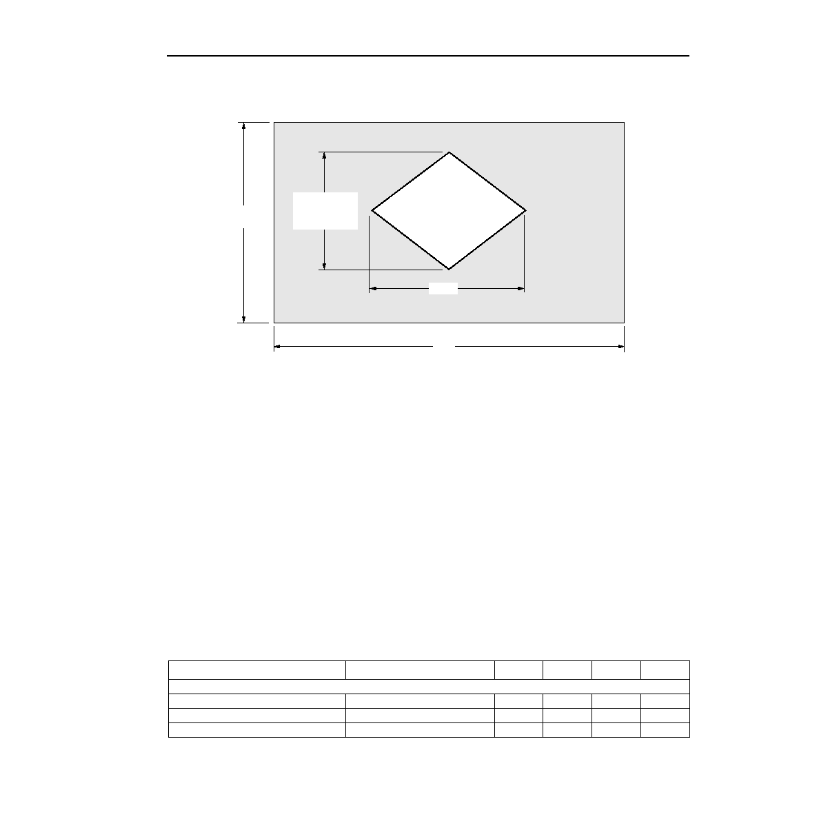
Figure 28. Receive Data Eye-Diagram Template (Differential)
Figure 28 provides a graphical characterization of the SERDES receiver input requirements. It provides guidance
on a number of input parameters, including signal amplitude and rise time limits, noise and jitter limits, and P and N
input skew tolerance. it is believed that incoming data patterns falling within the shaded region of the template will
be received without error (BER < 10E-12), over all specied operating conditions.
Data pattern eye-opening at the receive end of a link is considered the ultimate measures of received signal qual-
ity. Almost all detrimental characteristics of transmit signal and the interconnection link design result in eye-closure.
This combined with the eye-opening limitations of the line receiver can provide a good indication of a links ability to
transfer data error-free.
Signal jitter is of special interest to system designers. It is often the primary limiting characteristic of long digital
links and of systems with high noise level environments. An interesting characteristic of the clock and data recov-
ery (CDR) portion of the ORT82G5 SERDES receiver is its ability to lter incoming signal jitter that is below the
clock recovery PLL bandwidth (estimated to be about 3 MHz). For signals with high levels of low frequency jitter the
receiver can detect incoming data, error-free, with eye-openings signicantly less than that of Figure 28. This phe-
nomena has been observed in the laboratory.
Eye-diagram measurement and simulation are excellent tools of design. They are both highly recommended when
designing serial link interconnections and evaluating signal integrity.
Table 23. Receiver Specications
Parameter
Conditions
Min
Typ
Max
Unit
Input Data
Stream of Nontransitions
—
60
Bits
Eye Opening Interval
—
0.4
—
UIP-P
Eye Opening Voltage
—
200
—
mVP-P
0.4UI
200 mV
1.2 V
UI
相关PDF资料 |
PDF描述 |
|---|---|
| ORT82G5-3BM680 | FPGA, 1296 CLBS, 380000 GATES, PBGA680 |
| OS10040280G-012 | FIBER OPTIC RECEIVER, 1290-1600nm, PANEL MOUNT, FC/APC CONNECTOR |
| OT-WBSC-Y-A-10-X-9-M-3-05-FA | FIBER OPTIC SPLITTER/COUPLER, 1X2PORT, 10.0, PANEL MOUNT, FC/APC CONNECTOR |
| OT-WBSC-Y-A-50-13-9-F-1-05-FA | FIBER OPTIC SPLITTER/COUPLER, 1X2PORT, 50.0, PANEL MOUNT, FC/APC CONNECTOR |
| OT-WBSC-Y-A-50-X-9-O-1-99-SA | FIBER OPTIC SPLITTER/COUPLER, 1X2PORT, 50.0, PANEL MOUNT, SC/APC CONNECTOR |
相关代理商/技术参数 |
参数描述 |
|---|---|
| ORT82G5-2BM680C | 功能描述:FPGA - 现场可编程门阵列 10368 LUT 372 I/O RoHS:否 制造商:Altera Corporation 系列:Cyclone V E 栅极数量: 逻辑块数量:943 内嵌式块RAM - EBR:1956 kbit 输入/输出端数量:128 最大工作频率:800 MHz 工作电源电压:1.1 V 最大工作温度:+ 70 C 安装风格:SMD/SMT 封装 / 箱体:FBGA-256 |
| ORT82G5-2BM680I | 功能描述:FPGA - 现场可编程门阵列 10368 LUT 372 I/O RoHS:否 制造商:Altera Corporation 系列:Cyclone V E 栅极数量: 逻辑块数量:943 内嵌式块RAM - EBR:1956 kbit 输入/输出端数量:128 最大工作频率:800 MHz 工作电源电压:1.1 V 最大工作温度:+ 70 C 安装风格:SMD/SMT 封装 / 箱体:FBGA-256 |
| ORT82G5-2F680C | 功能描述:FPGA - 现场可编程门阵列 ORCA FPSC 2.7Gbits/s BP XCVR 643K RoHS:否 制造商:Altera Corporation 系列:Cyclone V E 栅极数量: 逻辑块数量:943 内嵌式块RAM - EBR:1956 kbit 输入/输出端数量:128 最大工作频率:800 MHz 工作电源电压:1.1 V 最大工作温度:+ 70 C 安装风格:SMD/SMT 封装 / 箱体:FBGA-256 |
| ORT82G5-2F680I | 功能描述:FPGA - 现场可编程门阵列 ORCA FPSC 2.7GBITS/s BP XCVR 643K RoHS:否 制造商:Altera Corporation 系列:Cyclone V E 栅极数量: 逻辑块数量:943 内嵌式块RAM - EBR:1956 kbit 输入/输出端数量:128 最大工作频率:800 MHz 工作电源电压:1.1 V 最大工作温度:+ 70 C 安装风格:SMD/SMT 封装 / 箱体:FBGA-256 |
| ORT82G5-2FN680C | 功能描述:FPGA - 现场可编程门阵列 ORCA FPSC 1.5V 3.7 G b Bpln Xcvr 643K Gt RoHS:否 制造商:Altera Corporation 系列:Cyclone V E 栅极数量: 逻辑块数量:943 内嵌式块RAM - EBR:1956 kbit 输入/输出端数量:128 最大工作频率:800 MHz 工作电源电压:1.1 V 最大工作温度:+ 70 C 安装风格:SMD/SMT 封装 / 箱体:FBGA-256 |
发布紧急采购,3分钟左右您将得到回复。