- 您现在的位置:买卖IC网 > PDF目录192300 > S29XS064R0PBHW010 (SPANSION LLC) 4M X 16 FLASH 1.8V PROM, 80 ns, PBGA44 PDF资料下载
参数资料
| 型号: | S29XS064R0PBHW010 |
| 厂商: | SPANSION LLC |
| 元件分类: | PROM |
| 英文描述: | 4M X 16 FLASH 1.8V PROM, 80 ns, PBGA44 |
| 封装: | 7.50 X 5 MM, LEAD FREE, FBGA-44 |
| 文件页数: | 11/65页 |
| 文件大小: | 2116K |
| 代理商: | S29XS064R0PBHW010 |
第1页第2页第3页第4页第5页第6页第7页第8页第9页第10页当前第11页第12页第13页第14页第15页第16页第17页第18页第19页第20页第21页第22页第23页第24页第25页第26页第27页第28页第29页第30页第31页第32页第33页第34页第35页第36页第37页第38页第39页第40页第41页第42页第43页第44页第45页第46页第47页第48页第49页第50页第51页第52页第53页第54页第55页第56页第57页第58页第59页第60页第61页第62页第63页第64页第65页
July 22, 2011 S29VS_XS064R_00_06
S29VS/XS-R MirrorBit
Flash Family
19
Da ta
Sh e e t
(Adv a n ce
In f o r m ation)
9.3.2
S29XS-R AADM Access
To burst read data from the memory array in AADM mode, the system must assert CE# to VIL, OE# must go
low with AVD# for one cycle while the upper address is valid. The rising edge of CLK when OE# and AVD#
are Low captures the upper 16 bits of address. The rising edge of CLK when OE# is High and AVD# is Low
latches the lower 16 bits of address. The data appears on A/DQ15 -A/DQ0 when CE# remains Low, after
OE# is Low and the synchronous access times are satisfied. The next data in the burst sequence is read on
each clock cycle that OE# and CE# remain Low.
Once OE# returns to VIH during a burst read the OE# no longer enables the outputs until after AVD# is at VIL
with OE# at VIH - which signals that address-low has been captured for the next burst access. This is so that
OE# at VIL may be used in conjunction with AVD# at VIL to indicate address-high on the A/DQ signals without
enabling the A/DQ outputs, thus avoiding data output contention with Address-high.
The device has a fixed internal address boundary that occurs every 128 words. A boundary crossing of one or
two additional wait states is required. The time the device is outputting data with the starting burst address not
divisible by eight, additional waits might be required.
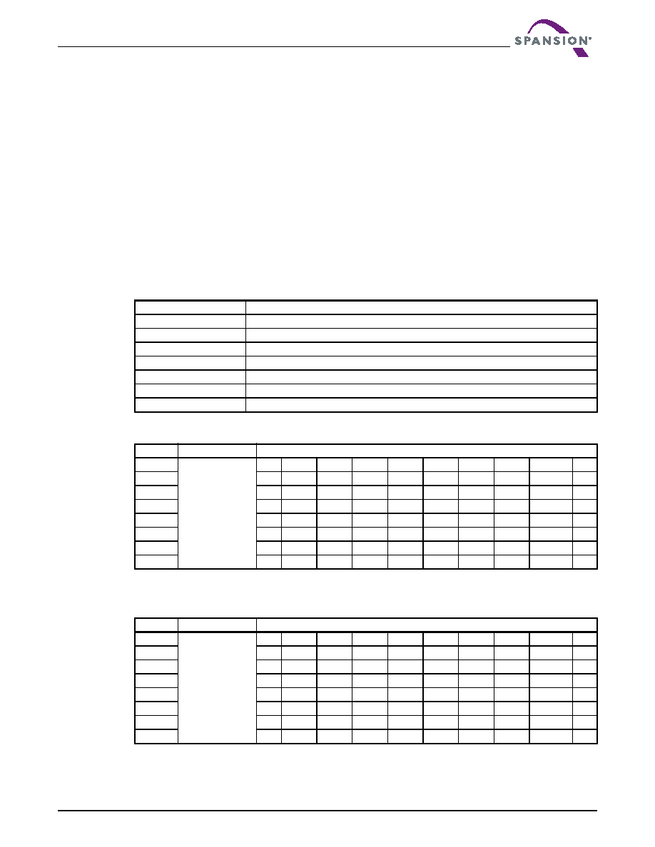
The following Tables show the latency for variable wait state operation (note that ws = wait state).
Table 9.2 Wait State vs. Frequency
Wait State
Frequency (Maximum MHz)
3
27
4
40
5
54
6
66
7
80
8
95
9
108
Table 9.3 Address Latency for 10 -13 Wait States
Word
Initial Wait
Subsequent Clock Cycles After Initial Wait States
0
10 -13 wait states
D0
D1
D2
D3
D4
D5
D6
D7
+2 ws
D8
1
D1
D2
D3D4D5D6D7
1 ws
+2 ws
D8
2
D2
D3
D4D5D6D7
1 ws
+2 ws
D8
3
D3
D4
D5
D6
D7
1 ws
+2 ws
D8
4
D4
D5
D6
D7
1 ws
+2 ws
D8
5
D5
D6
D7
1 ws
+2 ws
D8
6
D6
D7
1 ws
+2 ws
D8
7
D7
1 ws
+2 ws
D8
Table 9.4 Address Latency for 9 Wait States
Word
Initial Wait
Subsequent Clock Cycles After Initial Wait States
0
9 wait states
D0
D1
D2
D3
D4
D5
D6
D7
+1 ws
D8
1
D1
D2
D3D4D5D6D7
1 ws
+1 ws
D8
2
D2
D3
D4D5D6D7
1 ws
+1 ws
D8
3
D3
D4
D5
D6
D7
1 ws
+1 ws
D8
4
D4
D5
D6
D7
1 ws
+1 ws
D8
5
D5
D6
D7
1 ws
+1 ws
D8
6
D6
D7
1 ws
+1 ws
D8
7
D7
1 ws
+1 ws
D8
相关PDF资料 |
PDF描述 |
|---|---|
| S2C3R-1-12-H | 4000 MHz - 12000 MHz RF/MICROWAVE SGL POLE DOUBLE THROW SWITCH, 2 dB INSERTION LOSS |
| S2C5R-1-12-RC | 4000 MHz - 18000 MHz RF/MICROWAVE SGL POLE DOUBLE THROW SWITCH, 2.8 dB INSERTION LOSS |
| S2H3R-1H | 10 MHz - 1000 MHz RF/MICROWAVE SGL POLE DOUBLE THROW SWITCH, 1.2 dB INSERTION LOSS |
| S2L1R-RC | 1000 MHz - 2000 MHz RF/MICROWAVE SGL POLE DOUBLE THROW SWITCH, 0.9 dB INSERTION LOSS |
| S2L7R-1-RC | 1000 MHz - 18000 MHz RF/MICROWAVE SGL POLE DOUBLE THROW SWITCH, 2.9 dB INSERTION LOSS |
相关代理商/技术参数 |
参数描述 |
|---|---|
| S-29XX0A | 制造商:SII 制造商全称:Seiko Instruments Inc 功能描述:CMOS SERIAL EEPROM |
| S-29XX1A | 制造商:SII 制造商全称:Seiko Instruments Inc 功能描述:CMOS SERIAL EEPROM |
| S-29ZX30A | 制造商:未知厂家 制造商全称:未知厂家 功能描述:Serial 3-wire EEPROMs |
| S2A | 功能描述:拨动开关 ON-NONE-ON SPDT SOLDER LUG RoHS:否 制造商:C&K Components 触点形式:DPDT 开关功能:ON - ON - ON 电流额定值: 电压额定值 AC:20 V 电压额定值 DC:20 V 功率额定值:0.4 VA 端接类型:V-Bracket 安装风格: 端子密封:Epoxy 触点电镀:Gold 照明:Not Illuminated |
| S-2A | 制造商:Nihon Kaiheiki Ind Co Ltd 功能描述:30V 50000(@BIv) / 25000(dCIv) bL +85 -30 30mm 18mm 45.5mm Bulk 制造商:Nihon Dempa Kogyo Co (NDK) 功能描述:Switch, toggle, solder terminal, minitur |
发布紧急采购,3分钟左右您将得到回复。