- 您现在的位置:买卖IC网 > PDF目录192300 > S29XS064R0PBHW010 (SPANSION LLC) 4M X 16 FLASH 1.8V PROM, 80 ns, PBGA44 PDF资料下载
参数资料
| 型号: | S29XS064R0PBHW010 |
| 厂商: | SPANSION LLC |
| 元件分类: | PROM |
| 英文描述: | 4M X 16 FLASH 1.8V PROM, 80 ns, PBGA44 |
| 封装: | 7.50 X 5 MM, LEAD FREE, FBGA-44 |
| 文件页数: | 29/65页 |
| 文件大小: | 2116K |
| 代理商: | S29XS064R0PBHW010 |
第1页第2页第3页第4页第5页第6页第7页第8页第9页第10页第11页第12页第13页第14页第15页第16页第17页第18页第19页第20页第21页第22页第23页第24页第25页第26页第27页第28页当前第29页第30页第31页第32页第33页第34页第35页第36页第37页第38页第39页第40页第41页第42页第43页第44页第45页第46页第47页第48页第49页第50页第51页第52页第53页第54页第55页第56页第57页第58页第59页第60页第61页第62页第63页第64页第65页
July 22, 2011 S29VS_XS064R_00_06
S29VS/XS-R MirrorBit
Flash Family
35
Da ta
Sh e e t
(Adv a n ce
In f o r m ation)
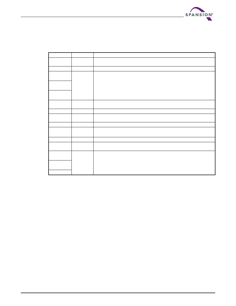
12. Configuration Register
Table 12.1 shows the address bits that determine the configuration register settings for various device
functions.
Notes
1. Device will be in the default state upon power-up or hardware reset.
2. CR3 will always equal to 1 (Wrap around mode) when CR0,CR1,CR2 = 000 (continuous Burst mode).
12.1
Reset Command
Writing the reset command resets the banks to the read or erase-suspend-read mode. Address bits are don’t
cares for this command.
The reset command may be written between the sequence cycles in an erase command sequence before
erasing begins. This resets the bank to which the system was writing to the read mode. Once erasure
begins, however, the device ignores reset commands until the operation is complete.
The reset command may be written between the sequence cycles in a program command sequence before
programming begins. This resets the bank to which the system was writing to the read mode. If the program
command sequence is written to a bank that is in the Erase Suspend mode, writing the reset command
returns that bank to the erase-suspend-read mode. Once programming begins, however, the device
ignores reset commands until the operation is complete.
The reset command may be written between the sequence cycles in an autoselect command sequence.
Once in the autoselect mode, the reset command must be written to return to the read mode. If a bank
entered the autoselect mode while in the Erase Suspend mode, writing the reset command returns that bank
to the erase-suspend-read mode.
If DQ5 goes high during a program or erase operation, writing the reset command returns the banks to the
read mode (or erase-suspend-read mode if that bank was in Erase Suspend).
Table 12.1 Configuration Register
CR BIt
Function
Settings (Binary)
CR15
Device Read
Mode
0 = Synchronous Read Mode
1 = Asynchronous Read Mode (Default)
CR14
Reserved
0 = Default
CR13
Programmable
Wait State
000 = Reserved
001 = Data is valid on the 3rd active CLK edge after addresses are latched
010 = Data is valid on the 4th active CLK edge after addresses are latched
011 = Data is valid on the 5th active CLK edge after addresses are latched
100 = Data is valid on the 6th active CLK edge after addresses are latched
101 = Data is valid on the 7th active CLK edge after addresses are latched (default)
110 = Data is valid on the 8th active CLK edge after addresses are latched
111 = Data is valid on the 9th active CLK edge after addresses are latched
CR12
CR11
CR10
RDY Polarity
0 = RDY signal is active low
1 = RDY signal is active high (default)
CR9
Reserved
1 = Default
CR8
RDY
0 = RDY active one clock cycle before data
1 = RDY active with data (default)
CR7
Reserved
1 = default
CR6
Reserved
1 = default
CR5
Reserved
0 = default
CR4
Reserved
0 = default
CR3
Burst Wrap
Around
0 = Reserved
1 = Wrap Around Burst (default)
CR2
Burst Length
000 = Continuous (default)
010 = 8-Word Linear Burst
011 = 16-Word Linear Burst
100 = Reserved
(All other bit settings are reserved)
CR1
CR0
相关PDF资料 |
PDF描述 |
|---|---|
| S2C3R-1-12-H | 4000 MHz - 12000 MHz RF/MICROWAVE SGL POLE DOUBLE THROW SWITCH, 2 dB INSERTION LOSS |
| S2C5R-1-12-RC | 4000 MHz - 18000 MHz RF/MICROWAVE SGL POLE DOUBLE THROW SWITCH, 2.8 dB INSERTION LOSS |
| S2H3R-1H | 10 MHz - 1000 MHz RF/MICROWAVE SGL POLE DOUBLE THROW SWITCH, 1.2 dB INSERTION LOSS |
| S2L1R-RC | 1000 MHz - 2000 MHz RF/MICROWAVE SGL POLE DOUBLE THROW SWITCH, 0.9 dB INSERTION LOSS |
| S2L7R-1-RC | 1000 MHz - 18000 MHz RF/MICROWAVE SGL POLE DOUBLE THROW SWITCH, 2.9 dB INSERTION LOSS |
相关代理商/技术参数 |
参数描述 |
|---|---|
| S-29XX0A | 制造商:SII 制造商全称:Seiko Instruments Inc 功能描述:CMOS SERIAL EEPROM |
| S-29XX1A | 制造商:SII 制造商全称:Seiko Instruments Inc 功能描述:CMOS SERIAL EEPROM |
| S-29ZX30A | 制造商:未知厂家 制造商全称:未知厂家 功能描述:Serial 3-wire EEPROMs |
| S2A | 功能描述:拨动开关 ON-NONE-ON SPDT SOLDER LUG RoHS:否 制造商:C&K Components 触点形式:DPDT 开关功能:ON - ON - ON 电流额定值: 电压额定值 AC:20 V 电压额定值 DC:20 V 功率额定值:0.4 VA 端接类型:V-Bracket 安装风格: 端子密封:Epoxy 触点电镀:Gold 照明:Not Illuminated |
| S-2A | 制造商:Nihon Kaiheiki Ind Co Ltd 功能描述:30V 50000(@BIv) / 25000(dCIv) bL +85 -30 30mm 18mm 45.5mm Bulk 制造商:Nihon Dempa Kogyo Co (NDK) 功能描述:Switch, toggle, solder terminal, minitur |
发布紧急采购,3分钟左右您将得到回复。