- 您现在的位置:买卖IC网 > PDF目录192300 > S29XS064R0PBHW010 (SPANSION LLC) 4M X 16 FLASH 1.8V PROM, 80 ns, PBGA44 PDF资料下载
参数资料
| 型号: | S29XS064R0PBHW010 |
| 厂商: | SPANSION LLC |
| 元件分类: | PROM |
| 英文描述: | 4M X 16 FLASH 1.8V PROM, 80 ns, PBGA44 |
| 封装: | 7.50 X 5 MM, LEAD FREE, FBGA-44 |
| 文件页数: | 39/65页 |
| 文件大小: | 2116K |
| 代理商: | S29XS064R0PBHW010 |
第1页第2页第3页第4页第5页第6页第7页第8页第9页第10页第11页第12页第13页第14页第15页第16页第17页第18页第19页第20页第21页第22页第23页第24页第25页第26页第27页第28页第29页第30页第31页第32页第33页第34页第35页第36页第37页第38页当前第39页第40页第41页第42页第43页第44页第45页第46页第47页第48页第49页第50页第51页第52页第53页第54页第55页第56页第57页第58页第59页第60页第61页第62页第63页第64页第65页
44
S29VS/XS-R MirrorBit
Flash Family
S29VS_XS064R_00_06 July 22, 2011
Data
Sheet
(Adv an ce
Inf o r m a t io n)
Legend
X = Don’t care
RA = Address of the memory location to be read.
RD = Data read from location RA during read operation.
PA = Address of the memory location to be programmed. Addresses latch on the falling edge of the WE# or CE# pulse, whichever happens
later.
PD = Data to be programmed at location PA. Data latches on the rising edge of WE# or CE# pulse, whichever happens first.
PD(0) = Secured Silicon Sector Lock Bit. PD(0), or bit[0].
PD(3) = Protection Mode OTP Bit. PD(3) or bit[3].
SA = Address of the sector to be verified (in autoselect mode) or erased. SA includes BA. Address bits Amax - A13 uniquely select any sector.
BA = Address of the bank A21-A19.
CR = Configuration Register set by data bits D15-D0.
RD(0) = DQ0 protection indicator bit. If protected, DQ0 = 0, if unprotected, DQ0 = 1.
RD(1) = DQ1 protection indicator bit. If protected, DQ1 = 0, if unprotected, DQ1 = 1.
RD(2) = DQ2 protection indicator bit. If protected, DQ2 = 0, if unprotected, DQ2 = 1.
RD(4) = DQ4 protection indicator bit. If protected, DQ4 = 0, if unprotected, DQ4 = 1.
WBL = Write Buffer Location. Address must be within the same write buffer page as PA.
WC = Word Count. Number of write buffer locations to load minus 1.
Notes
1. See Table 9.1 for description of bus operations.
2. All values are in hexadecimal.
3. Except for the read cycle and the fourth cycle of the autoselect command sequence, all bus cycles are write cycles.
4. Data bits DQ15–DQ8 are don’t care in command sequences, except for RD and PD.
5. Unless otherwise noted, address bits Amax–A12 are don’t cares.
6. Writing incorrect address and data values or writing them in the improper sequence may place the device in an unknown state. The
system must write the reset command to return the device to reading array data.
7. No unlock or command cycles required when bank is reading array data.
8. The Reset command is required to return to reading array data (or to the erase-suspend-read mode if previously in Erase Suspend) when
a bank is in the autoselect mode, or if DQ5 goes high (while the bank is providing status information).
9. The fourth cycle of the autoselect command sequence is a read cycle. The system must read device IDs across the 4th, 5th, and 6th
cycles, The system must provide the bank address. See Autoselect Command Sequence on page 36 for more information.
10.
See Table 9.1 for description of bus operations.
11. See the Autoselect Command Sequence on page 36.
12. The system may read and program in non-erasing sectors, or enter the autoselect mode, when in the Erase Suspend mode. The Erase
Suspend command is valid only during a sector erase operation, and requires the bank address.
13. The Erase Resume command is valid only during the Erase Suspend mode, and requires the bank address.
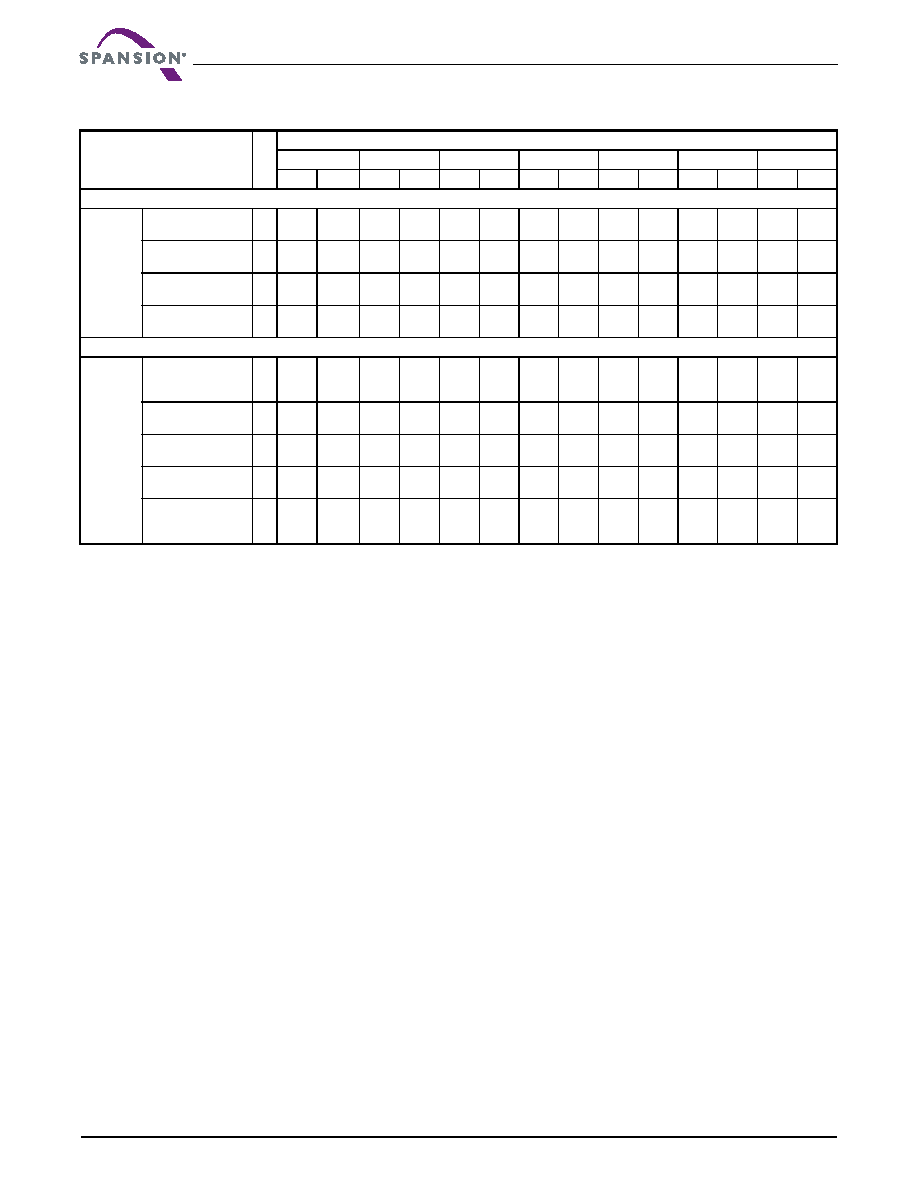
Secured Silicon Sector Command Definitions
S
e
cured
Si
licon
Sect
or
Secured Silicon
Sector Entry
3
555
AA
2AA
55
555
88
Secured Silicon
Sector Program
2XX
A0
PA
data
Secured Silicon
Sector Read
1
RA
data
Secured Silicon
Sector Exit
4
555
AA
2AA
55
555
90
XX
00
Volatile Sector Protection Command Set Definitions
DYB
Volatile Sector
Protection Command
Set Entry (17)
3
555
AA
2AA
55
(BA)
555
E0
DYB Set
2
XX
A0
(BA)
SA
00
DYB Clear
2
XX
A0
(BA)
SA
01
DYB Status Read
1
(BA)
SA
RD(0)
Volatile Sector
Protection Command
Set Exit
2XX
90
XX
00
Table 12.3 Command Definitions (Sheet 2 of 2)
Command Sequence
(Notes)
Cy
c
les
Bus Cycles (Notes 1–6)
First
Second
Third
Fourth
Fifth
Sixth
Seventh
Addr
Data
Addr
Data
Addr
Data
Addr
Data
Addr
Data
Addr
Data
Addr
Data
相关PDF资料 |
PDF描述 |
|---|---|
| S2C3R-1-12-H | 4000 MHz - 12000 MHz RF/MICROWAVE SGL POLE DOUBLE THROW SWITCH, 2 dB INSERTION LOSS |
| S2C5R-1-12-RC | 4000 MHz - 18000 MHz RF/MICROWAVE SGL POLE DOUBLE THROW SWITCH, 2.8 dB INSERTION LOSS |
| S2H3R-1H | 10 MHz - 1000 MHz RF/MICROWAVE SGL POLE DOUBLE THROW SWITCH, 1.2 dB INSERTION LOSS |
| S2L1R-RC | 1000 MHz - 2000 MHz RF/MICROWAVE SGL POLE DOUBLE THROW SWITCH, 0.9 dB INSERTION LOSS |
| S2L7R-1-RC | 1000 MHz - 18000 MHz RF/MICROWAVE SGL POLE DOUBLE THROW SWITCH, 2.9 dB INSERTION LOSS |
相关代理商/技术参数 |
参数描述 |
|---|---|
| S-29XX0A | 制造商:SII 制造商全称:Seiko Instruments Inc 功能描述:CMOS SERIAL EEPROM |
| S-29XX1A | 制造商:SII 制造商全称:Seiko Instruments Inc 功能描述:CMOS SERIAL EEPROM |
| S-29ZX30A | 制造商:未知厂家 制造商全称:未知厂家 功能描述:Serial 3-wire EEPROMs |
| S2A | 功能描述:拨动开关 ON-NONE-ON SPDT SOLDER LUG RoHS:否 制造商:C&K Components 触点形式:DPDT 开关功能:ON - ON - ON 电流额定值: 电压额定值 AC:20 V 电压额定值 DC:20 V 功率额定值:0.4 VA 端接类型:V-Bracket 安装风格: 端子密封:Epoxy 触点电镀:Gold 照明:Not Illuminated |
| S-2A | 制造商:Nihon Kaiheiki Ind Co Ltd 功能描述:30V 50000(@BIv) / 25000(dCIv) bL +85 -30 30mm 18mm 45.5mm Bulk 制造商:Nihon Dempa Kogyo Co (NDK) 功能描述:Switch, toggle, solder terminal, minitur |
发布紧急采购,3分钟左右您将得到回复。