- 您现在的位置:买卖IC网 > PDF目录192300 > S29XS064R0PBHW010 (SPANSION LLC) 4M X 16 FLASH 1.8V PROM, 80 ns, PBGA44 PDF资料下载
参数资料
| 型号: | S29XS064R0PBHW010 |
| 厂商: | SPANSION LLC |
| 元件分类: | PROM |
| 英文描述: | 4M X 16 FLASH 1.8V PROM, 80 ns, PBGA44 |
| 封装: | 7.50 X 5 MM, LEAD FREE, FBGA-44 |
| 文件页数: | 9/65页 |
| 文件大小: | 2116K |
| 代理商: | S29XS064R0PBHW010 |
第1页第2页第3页第4页第5页第6页第7页第8页当前第9页第10页第11页第12页第13页第14页第15页第16页第17页第18页第19页第20页第21页第22页第23页第24页第25页第26页第27页第28页第29页第30页第31页第32页第33页第34页第35页第36页第37页第38页第39页第40页第41页第42页第43页第44页第45页第46页第47页第48页第49页第50页第51页第52页第53页第54页第55页第56页第57页第58页第59页第60页第61页第62页第63页第64页第65页
July 22, 2011 S29VS_XS064R_00_06
S29VS/XS-R MirrorBit
Flash Family
17
Da ta
Sh e e t
(Adv a n ce
In f o r m ation)
The upper address is set to Zero or all Ones, for bottom or top boot respectively, during a Hardware Reset,
operate in ADM mode during the early phase of boot code execution where only a single address cycle would
be issued with the lower 16 bit of the address reaching the memory in AADM mode. The default high order
address bits will direct the early boot accesses to the 128 Kbytes at the boot end of the device. Note that in
AADM interface mode this effectively requires that one of the boot sectors is selected for any address overlay
mode because in the initial phase of AADM mode operation the host memory controller may only issue the
low order address thus limiting the early boot time address space to the 128 Kbytes at the boot end of the
device.
8.3
Default Access Mode
Upon power-up or hardware reset, the device defaults to the Asynchronous Access mode.
9.
Device Bus Operations
This section describes the requirements and use of the device bus operations, which are initiated through the
internal command register. The command register itself does not occupy any addressable memory location.
The register is composed of latches that store the commands, along with the address and data information
needed to execute the command. The contents of the register serve as inputs to the internal state machine.
The state machine outputs dictate the function of the device. Table 9.1 lists the device bus operations, the
inputs and control levels they require, and the resulting output. The following subsections describe each of
these operations in further detail.
Legend
L = Logic 0, H = Logic 1, X = Don’t Care.
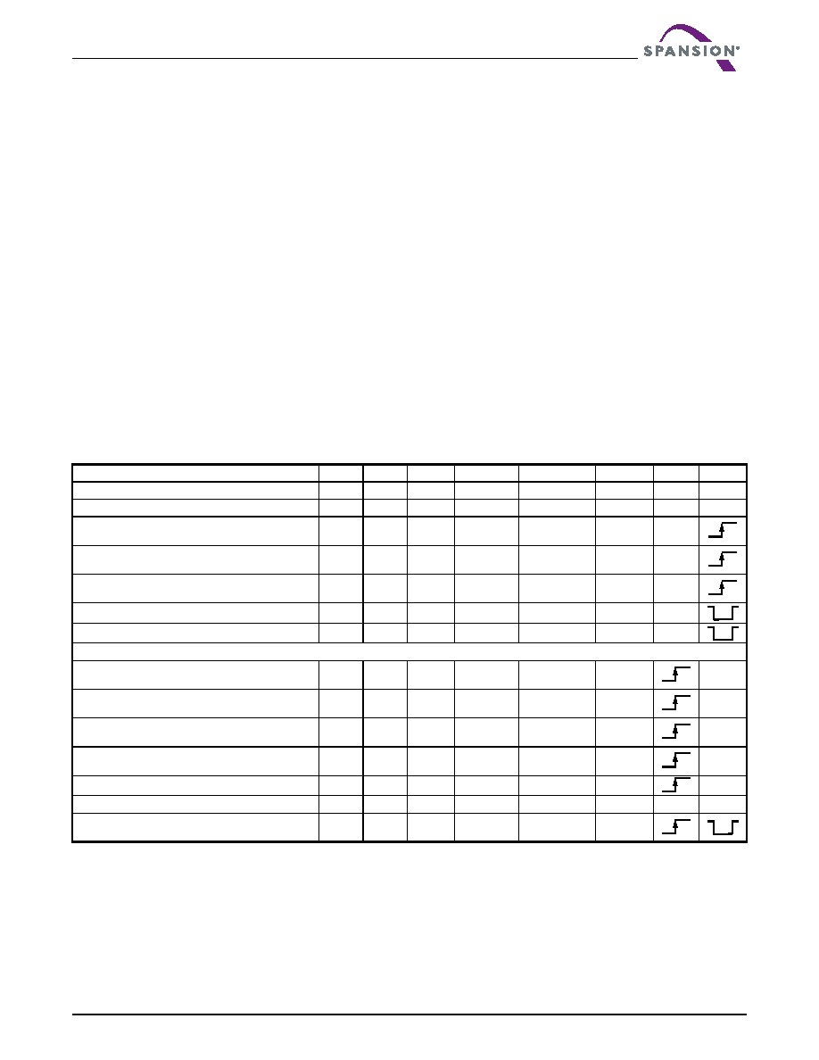
Table 9.1 Device Bus Operations
Operation
CE#
OE#
WE#
Amax–16
A/DQ15–0
RESET#
CLK
AVD#
Standby (CE#)
H
X
High-Z
H
H/L
X
Hardware Reset
X
High-Z
L
X
Asynchronous Address Latch
- ADM mode (29VS064R only)
L
H
X
Addr In
H
X
Asynchronous Upper Address Latch
- AADM mode (29XS064R only)
L
H
X
Addr In
H
X
Asynchronous Lower Address Latch
- AADM mode (29XS064R only)
L
H
X
Addr In
H
X
Asynchronous Read
L
H
Addr In
I/O
H
L
Write
L
H
L
Addr In
I/O
H
H/L
Burst Read Operations
Latch Starting Burst Address by CLK
-ADM mode (29VS064R only)
L
H
Addr In
H
L
Latch Upper Starting Burst Address by CLK -AADM mode
(29XS064R only)
L
H
X
Addr In
H
L
Latch Lower Starting Burst Address by CLK -AADM mode
(29XS064R only)
L
H
X
Addr In
H
L
Advance Burst to next address with appropriate Data
presented on the Data Bus
LL
H
X
Burst
Data Out
HH
Terminate current Burst read cycle
H
X
H
X
High-Z
H
X
Terminate current Burst read cycle via RESET#
X
H
X
High-Z
L
X
Terminate current Burst read cycle and start new Burst
read cycle
L
H
X
I/O
H
相关PDF资料 |
PDF描述 |
|---|---|
| S2C3R-1-12-H | 4000 MHz - 12000 MHz RF/MICROWAVE SGL POLE DOUBLE THROW SWITCH, 2 dB INSERTION LOSS |
| S2C5R-1-12-RC | 4000 MHz - 18000 MHz RF/MICROWAVE SGL POLE DOUBLE THROW SWITCH, 2.8 dB INSERTION LOSS |
| S2H3R-1H | 10 MHz - 1000 MHz RF/MICROWAVE SGL POLE DOUBLE THROW SWITCH, 1.2 dB INSERTION LOSS |
| S2L1R-RC | 1000 MHz - 2000 MHz RF/MICROWAVE SGL POLE DOUBLE THROW SWITCH, 0.9 dB INSERTION LOSS |
| S2L7R-1-RC | 1000 MHz - 18000 MHz RF/MICROWAVE SGL POLE DOUBLE THROW SWITCH, 2.9 dB INSERTION LOSS |
相关代理商/技术参数 |
参数描述 |
|---|---|
| S-29XX0A | 制造商:SII 制造商全称:Seiko Instruments Inc 功能描述:CMOS SERIAL EEPROM |
| S-29XX1A | 制造商:SII 制造商全称:Seiko Instruments Inc 功能描述:CMOS SERIAL EEPROM |
| S-29ZX30A | 制造商:未知厂家 制造商全称:未知厂家 功能描述:Serial 3-wire EEPROMs |
| S2A | 功能描述:拨动开关 ON-NONE-ON SPDT SOLDER LUG RoHS:否 制造商:C&K Components 触点形式:DPDT 开关功能:ON - ON - ON 电流额定值: 电压额定值 AC:20 V 电压额定值 DC:20 V 功率额定值:0.4 VA 端接类型:V-Bracket 安装风格: 端子密封:Epoxy 触点电镀:Gold 照明:Not Illuminated |
| S-2A | 制造商:Nihon Kaiheiki Ind Co Ltd 功能描述:30V 50000(@BIv) / 25000(dCIv) bL +85 -30 30mm 18mm 45.5mm Bulk 制造商:Nihon Dempa Kogyo Co (NDK) 功能描述:Switch, toggle, solder terminal, minitur |
发布紧急采购,3分钟左右您将得到回复。