- 您现在的位置:买卖IC网 > PDF目录192300 > S29XS064R0PBHW010 (SPANSION LLC) 4M X 16 FLASH 1.8V PROM, 80 ns, PBGA44 PDF资料下载
参数资料
| 型号: | S29XS064R0PBHW010 |
| 厂商: | SPANSION LLC |
| 元件分类: | PROM |
| 英文描述: | 4M X 16 FLASH 1.8V PROM, 80 ns, PBGA44 |
| 封装: | 7.50 X 5 MM, LEAD FREE, FBGA-44 |
| 文件页数: | 31/65页 |
| 文件大小: | 2116K |
| 代理商: | S29XS064R0PBHW010 |
第1页第2页第3页第4页第5页第6页第7页第8页第9页第10页第11页第12页第13页第14页第15页第16页第17页第18页第19页第20页第21页第22页第23页第24页第25页第26页第27页第28页第29页第30页当前第31页第32页第33页第34页第35页第36页第37页第38页第39页第40页第41页第42页第43页第44页第45页第46页第47页第48页第49页第50页第51页第52页第53页第54页第55页第56页第57页第58页第59页第60页第61页第62页第63页第64页第65页
July 22, 2011 S29VS_XS064R_00_06
S29VS/XS-R MirrorBit
Flash Family
37
Da ta
Sh e e t
(Adv a n ce
In f o r m ation)
12.4
Program Command Sequence
Programming is a four-bus-cycle operation. The program command sequence is initiated by writing two
unlock write cycles, followed by the program set-up command. The program address and data are written
next, which in turn initiate the Embedded Program algorithm. The system is not required to provide further
controls or timings. The device automatically provides internally generated program pulses and verifies the
programmed cell margin. Table 12.3 on page 43 shows the address and data requirements for the program
command sequence.
When the Embedded Program algorithm is complete, that bank then returns to the read mode and addresses
are no longer latched. The system can determine the status of the program operation by monitoring DQ7 or
DQ6/DQ2. Refer to Write Operation Status on page 45 for information on these status bits.
Any commands written to the device during the Embedded Program Algorithm are ignored. Note that a
hardware reset immediately terminates the program operation. The program command sequence should be
reinitiated once that bank has returned to the read mode, to ensure data integrity.
Programming is allowed in any sequence and across sector boundaries. A bit cannot be programmed from
“0” back to a “1.” Attempting to do so may causes that bank to set DQ5 = 1 (change-up condition). However,
a succeeding read will show that the data is still “0.” Only erase operations can convert a “0” to a “1.”
12.5
Accelerated Program
The device offers accelerated program operations through the VPP input. The device uses the higher voltage
on the VPP input to accelerate the operation.
Figure 12.1 illustrates the algorithm for the program operation. Refer to the Erase/Program Operations table
in AC Characteristics for parameters, and Figure 19.6, on page 59 for timing diagrams.
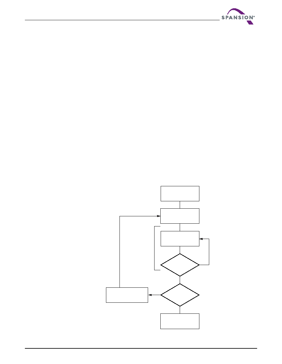
Figure 12.1 Program Operation
Note
1. See Table 12.3 on page 43 for program command sequence.
START
Write Program
Command Sequence
Data Poll
from System
Verify Data?
No
Yes
Last Address?
No
Yes
Programming
Completed
Increment Address
Embedded
Program
algorithm
in progress
相关PDF资料 |
PDF描述 |
|---|---|
| S2C3R-1-12-H | 4000 MHz - 12000 MHz RF/MICROWAVE SGL POLE DOUBLE THROW SWITCH, 2 dB INSERTION LOSS |
| S2C5R-1-12-RC | 4000 MHz - 18000 MHz RF/MICROWAVE SGL POLE DOUBLE THROW SWITCH, 2.8 dB INSERTION LOSS |
| S2H3R-1H | 10 MHz - 1000 MHz RF/MICROWAVE SGL POLE DOUBLE THROW SWITCH, 1.2 dB INSERTION LOSS |
| S2L1R-RC | 1000 MHz - 2000 MHz RF/MICROWAVE SGL POLE DOUBLE THROW SWITCH, 0.9 dB INSERTION LOSS |
| S2L7R-1-RC | 1000 MHz - 18000 MHz RF/MICROWAVE SGL POLE DOUBLE THROW SWITCH, 2.9 dB INSERTION LOSS |
相关代理商/技术参数 |
参数描述 |
|---|---|
| S-29XX0A | 制造商:SII 制造商全称:Seiko Instruments Inc 功能描述:CMOS SERIAL EEPROM |
| S-29XX1A | 制造商:SII 制造商全称:Seiko Instruments Inc 功能描述:CMOS SERIAL EEPROM |
| S-29ZX30A | 制造商:未知厂家 制造商全称:未知厂家 功能描述:Serial 3-wire EEPROMs |
| S2A | 功能描述:拨动开关 ON-NONE-ON SPDT SOLDER LUG RoHS:否 制造商:C&K Components 触点形式:DPDT 开关功能:ON - ON - ON 电流额定值: 电压额定值 AC:20 V 电压额定值 DC:20 V 功率额定值:0.4 VA 端接类型:V-Bracket 安装风格: 端子密封:Epoxy 触点电镀:Gold 照明:Not Illuminated |
| S-2A | 制造商:Nihon Kaiheiki Ind Co Ltd 功能描述:30V 50000(@BIv) / 25000(dCIv) bL +85 -30 30mm 18mm 45.5mm Bulk 制造商:Nihon Dempa Kogyo Co (NDK) 功能描述:Switch, toggle, solder terminal, minitur |
发布紧急采购,3分钟左右您将得到回复。