- 您现在的位置:买卖IC网 > PDF目录192300 > S29XS064R0PBHW010 (SPANSION LLC) 4M X 16 FLASH 1.8V PROM, 80 ns, PBGA44 PDF资料下载
参数资料
| 型号: | S29XS064R0PBHW010 |
| 厂商: | SPANSION LLC |
| 元件分类: | PROM |
| 英文描述: | 4M X 16 FLASH 1.8V PROM, 80 ns, PBGA44 |
| 封装: | 7.50 X 5 MM, LEAD FREE, FBGA-44 |
| 文件页数: | 14/65页 |
| 文件大小: | 2116K |
| 代理商: | S29XS064R0PBHW010 |
第1页第2页第3页第4页第5页第6页第7页第8页第9页第10页第11页第12页第13页当前第14页第15页第16页第17页第18页第19页第20页第21页第22页第23页第24页第25页第26页第27页第28页第29页第30页第31页第32页第33页第34页第35页第36页第37页第38页第39页第40页第41页第42页第43页第44页第45页第46页第47页第48页第49页第50页第51页第52页第53页第54页第55页第56页第57页第58页第59页第60页第61页第62页第63页第64页第65页
July 22, 2011 S29VS_XS064R_00_06
S29VS/XS-R MirrorBit
Flash Family
21
Da ta
Sh e e t
(Adv a n ce
In f o r m ation)
The device will continue to output continuous, sequential burst data, wrapping around to address 000000h
after it reaches the highest addressable memory location, until the system asserts CE# high, RESET# low, or
AVD# low in conjunction with a new address. See Table 9.1 on page 17. The reset command does not
terminate the burst read operation.
8- and 16-Word Linear Burst with Wrap Around
These two modes are of the linear wrap around design, in which a fixed number of words are read from
consecutive addresses. In each of these modes, the burst addresses read are determined by the group within
which the starting address falls. The groups are sized according to the number of words read in a single burst
sequence for a given mode (see Table 9.11.)
As an example: if the starting address in the 8-word mode is 3Ah, and the burst sequence would be 3A-3B-
3C-3D-3E-3F-38-39h. The burst sequence begins with the starting address written to the device, but wraps
back to the first address in the selected group. In a similar fashion, the 16-word Linear Wrap mode begins its
burst sequence on the starting address written to the device, and then wraps back to the first address in the
selected address group and terminates the burst read. Note that in these two burst read modes the
address pointer does not cross the boundary that occurs every 128 words; thus, no wait states are
inserted (except during the initial access).
9.4
Programmable Wait State
The programmable wait state feature indicates to the device the number of additional clock cycles that must
elapse after AVD# is driven active before data will be available. Upon power up, the device defaults to the
maximum of seven total cycles. The total number of wait states is programmable from three to nine cycles.
For further details, see Set Configuration Register Command Sequence on page 32.
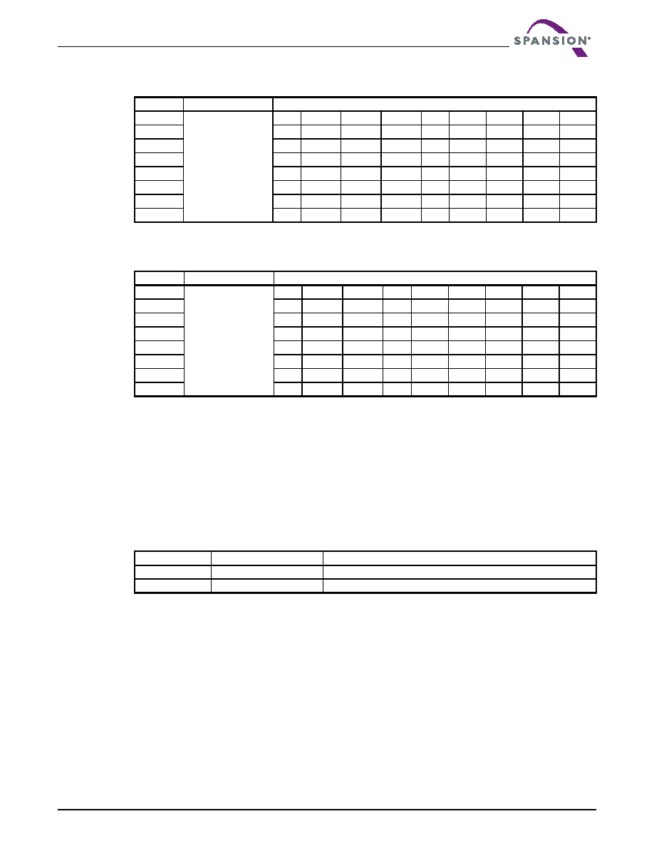
Table 9.9 Address Latency for 4 Wait States
Word
Initial Wait
Subsequent Clock Cycles After Initial Wait States
0
4 wait states
D0
D1
D2
D3
D4
D5
D6
D7
D8
1
D1D2
D3
D4D5
D6
D7
D8
D9
2
D2D3
D4
D5D6
D7
D8
D9
D10
3
D3D4
D5
D6D7
D8
D9
D10
D11
4
D4D5
D6
D7D8
D9
D10
D11
D12
5
D5
D6
D7
1 ws
D8
D9
D10
D11
D12
6
D6
D7
1 ws
D8
D9
D10
D11
D12
7
D7
1 ws
D8
D9
D10
D11
D12
Table 9.10 Address Latency for 3 Wait States
Word
Initial Wait
Subsequent Clock Cycles After Initial Wait States
0
3 wait states
D0
D1
D2
D3
D4
D5
D6
D7
D8
1
D1
D2
D3
D4
D5D6D7D8D9
2
D2
D3
D4
D5
D6D7D8D9
D10
3
D3D4
D5D6
D7
D8
D9
D10
D11
4
D4D5
D6D7
D8
D9
D10
D11
D12
5
D5D6
D7D8
D9
D10
D11
D12
D13
6
D6
D7
1 ws
D8
D9
D10
D11
D12
D13
7
D7
1 ws
D8
D9
D10
D11
D12
D13
Table 9.11 Burst Address Groups
Mode
Group Size
Group Address Ranges
8-word
8 words
0-7h, 8-Fh, 10-17h, 18-1Fh...
16-word
16 words
0-Fh, 10-1Fh, 20-2Fh, 30-3Fh...
相关PDF资料 |
PDF描述 |
|---|---|
| S2C3R-1-12-H | 4000 MHz - 12000 MHz RF/MICROWAVE SGL POLE DOUBLE THROW SWITCH, 2 dB INSERTION LOSS |
| S2C5R-1-12-RC | 4000 MHz - 18000 MHz RF/MICROWAVE SGL POLE DOUBLE THROW SWITCH, 2.8 dB INSERTION LOSS |
| S2H3R-1H | 10 MHz - 1000 MHz RF/MICROWAVE SGL POLE DOUBLE THROW SWITCH, 1.2 dB INSERTION LOSS |
| S2L1R-RC | 1000 MHz - 2000 MHz RF/MICROWAVE SGL POLE DOUBLE THROW SWITCH, 0.9 dB INSERTION LOSS |
| S2L7R-1-RC | 1000 MHz - 18000 MHz RF/MICROWAVE SGL POLE DOUBLE THROW SWITCH, 2.9 dB INSERTION LOSS |
相关代理商/技术参数 |
参数描述 |
|---|---|
| S-29XX0A | 制造商:SII 制造商全称:Seiko Instruments Inc 功能描述:CMOS SERIAL EEPROM |
| S-29XX1A | 制造商:SII 制造商全称:Seiko Instruments Inc 功能描述:CMOS SERIAL EEPROM |
| S-29ZX30A | 制造商:未知厂家 制造商全称:未知厂家 功能描述:Serial 3-wire EEPROMs |
| S2A | 功能描述:拨动开关 ON-NONE-ON SPDT SOLDER LUG RoHS:否 制造商:C&K Components 触点形式:DPDT 开关功能:ON - ON - ON 电流额定值: 电压额定值 AC:20 V 电压额定值 DC:20 V 功率额定值:0.4 VA 端接类型:V-Bracket 安装风格: 端子密封:Epoxy 触点电镀:Gold 照明:Not Illuminated |
| S-2A | 制造商:Nihon Kaiheiki Ind Co Ltd 功能描述:30V 50000(@BIv) / 25000(dCIv) bL +85 -30 30mm 18mm 45.5mm Bulk 制造商:Nihon Dempa Kogyo Co (NDK) 功能描述:Switch, toggle, solder terminal, minitur |
发布紧急采购,3分钟左右您将得到回复。