- 您现在的位置:买卖IC网 > PDF目录192300 > S29XS064R0PBHW010 (SPANSION LLC) 4M X 16 FLASH 1.8V PROM, 80 ns, PBGA44 PDF资料下载
参数资料
| 型号: | S29XS064R0PBHW010 |
| 厂商: | SPANSION LLC |
| 元件分类: | PROM |
| 英文描述: | 4M X 16 FLASH 1.8V PROM, 80 ns, PBGA44 |
| 封装: | 7.50 X 5 MM, LEAD FREE, FBGA-44 |
| 文件页数: | 27/65页 |
| 文件大小: | 2116K |
| 代理商: | S29XS064R0PBHW010 |
第1页第2页第3页第4页第5页第6页第7页第8页第9页第10页第11页第12页第13页第14页第15页第16页第17页第18页第19页第20页第21页第22页第23页第24页第25页第26页当前第27页第28页第29页第30页第31页第32页第33页第34页第35页第36页第37页第38页第39页第40页第41页第42页第43页第44页第45页第46页第47页第48页第49页第50页第51页第52页第53页第54页第55页第56页第57页第58页第59页第60页第61页第62页第63页第64页第65页
July 22, 2011 S29VS_XS064R_00_06
S29VS/XS-R MirrorBit
Flash Family
33
Da ta
Sh e e t
(Adv a n ce
In f o r m ation)
11.3.2
Programmable Wait State Configuration
The programmable wait state feature informs the device of the number of clock cycles that must elapse after
AVD# is driven active before data will be available. This value is determined by the input frequency of the
device. Configuration Bit CR13–CR11 determine the setting (see Table 11.1).
The wait state command sequence instructs the device to set a particular number of clock cycles for the initial
access in burst mode. The number of wait states that should be programmed into the device is directly related
to the clock frequency.
Notes
1. Upon power-up or hardware reset, the default setting is seven wait states.
2. RDY will default to being active with data when the Wait State Setting is set to a total initial access cycle of 2.
It is recommended that the wait state command sequence be written, even if the default wait state value is
desired, to ensure the device is set as expected. A hardware reset will set the wait state to the default setting.
11.3.3
Programmable Wait State
The host system should set CR13-CR11 to 100 for a clock frequency of 66 MHz for the system/device to
execute at maximum speed.
Table 11.2 describes the typical number of clock cycles (wait states) for various conditions.
11.3.4
Handshaking
For optimal burst mode performance, the host system must set the appropriate number of wait states in the
flash device depending on the clock frequency.
The autoselect function allows the host system to determine whether the flash device is enabled for
handshaking.
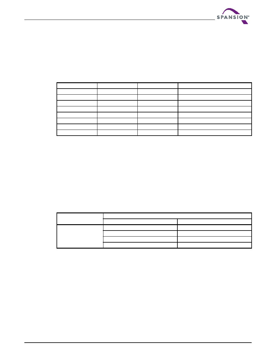
Table 11.1 Programmable Wait State Settings
CR13
CR12
CR11
Total Initial Access Cycles
000
Reserved
001
3
010
4
011
5
100
6
1
0
1
7 (default)
110
8
111
9
Table 11.2 Wait States for Handshaking
Conditions at Address
Typical No. of Clock Cycles after AVD# Low
Clock Cycles
Frequency (Maximum MHz)
Initial address (VCCQ = 1.8 V)
666
780
895
9
108
相关PDF资料 |
PDF描述 |
|---|---|
| S2C3R-1-12-H | 4000 MHz - 12000 MHz RF/MICROWAVE SGL POLE DOUBLE THROW SWITCH, 2 dB INSERTION LOSS |
| S2C5R-1-12-RC | 4000 MHz - 18000 MHz RF/MICROWAVE SGL POLE DOUBLE THROW SWITCH, 2.8 dB INSERTION LOSS |
| S2H3R-1H | 10 MHz - 1000 MHz RF/MICROWAVE SGL POLE DOUBLE THROW SWITCH, 1.2 dB INSERTION LOSS |
| S2L1R-RC | 1000 MHz - 2000 MHz RF/MICROWAVE SGL POLE DOUBLE THROW SWITCH, 0.9 dB INSERTION LOSS |
| S2L7R-1-RC | 1000 MHz - 18000 MHz RF/MICROWAVE SGL POLE DOUBLE THROW SWITCH, 2.9 dB INSERTION LOSS |
相关代理商/技术参数 |
参数描述 |
|---|---|
| S-29XX0A | 制造商:SII 制造商全称:Seiko Instruments Inc 功能描述:CMOS SERIAL EEPROM |
| S-29XX1A | 制造商:SII 制造商全称:Seiko Instruments Inc 功能描述:CMOS SERIAL EEPROM |
| S-29ZX30A | 制造商:未知厂家 制造商全称:未知厂家 功能描述:Serial 3-wire EEPROMs |
| S2A | 功能描述:拨动开关 ON-NONE-ON SPDT SOLDER LUG RoHS:否 制造商:C&K Components 触点形式:DPDT 开关功能:ON - ON - ON 电流额定值: 电压额定值 AC:20 V 电压额定值 DC:20 V 功率额定值:0.4 VA 端接类型:V-Bracket 安装风格: 端子密封:Epoxy 触点电镀:Gold 照明:Not Illuminated |
| S-2A | 制造商:Nihon Kaiheiki Ind Co Ltd 功能描述:30V 50000(@BIv) / 25000(dCIv) bL +85 -30 30mm 18mm 45.5mm Bulk 制造商:Nihon Dempa Kogyo Co (NDK) 功能描述:Switch, toggle, solder terminal, minitur |
发布紧急采购,3分钟左右您将得到回复。