- 您现在的位置:买卖IC网 > Datasheet目录369 > W9725G6JB25I (Winbond Electronics)IC DDR2 SDRAM 256MBIT 84WBGA Datasheet资料下载
参数资料
| 型号: | W9725G6JB25I |
| 厂商: | Winbond Electronics |
| 文件页数: | 47/87页 |
| 文件大小: | 0K |
| 描述: | IC DDR2 SDRAM 256MBIT 84WBGA |
| 标准包装: | 200 |
| 格式 - 存储器: | RAM |
| 存储器类型: | DDR2 SDRAM |
| 存储容量: | 256M(16Mx16) |
| 速度: | 2.5ns |
| 接口: | 并联 |
| 电源电压: | 1.7 V ~ 1.9 V |
| 工作温度: | -40°C ~ 95°C |
| 封装/外壳: | 84-TFBGA |
| 供应商设备封装: | 84-WBGA(8x12.5) |
| 包装: | 托盘 |
第1页第2页第3页第4页第5页第6页第7页第8页第9页第10页第11页第12页第13页第14页第15页第16页第17页第18页第19页第20页第21页第22页第23页第24页第25页第26页第27页第28页第29页第30页第31页第32页第33页第34页第35页第36页第37页第38页第39页第40页第41页第42页第43页第44页第45页第46页当前第47页第48页第49页第50页第51页第52页第53页第54页第55页第56页第57页第58页第59页第60页第61页第62页第63页第64页第65页第66页第67页第68页第69页第70页第71页第72页第73页第74页第75页第76页第77页第78页第79页第80页第81页第82页第83页第84页第85页第86页第87页
�� �
�
�W9725G6JB�
�Notes:�
�1.� All� voltages� are� referenced� to� V� SS� .�
�2.� Tests� for� AC� timing,� I� DD� ,� and� electrical� AC� and� DC� characteristics� may� be� conducted� at� nominal� reference/supply� voltage�
�levels,� but� the� related� specifications� and� device� operation� are� guaranteed� for� the� full� voltage� range� specified.� ODT� is�
�disabled� for� all� measurements� that� are� not� ODT-specific.�
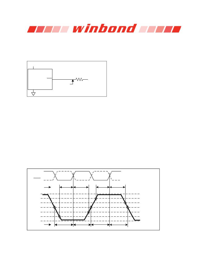
�3.� AC� timing� reference� load:�
�VDDQ�
�DQ�
�Output�
�DUT�
�DQS,� DQS�
�Figure� 16�
�Timing�
�25� Ω�
�reference�
�point�
�–� AC� timing� reference� load�
�VTT� =� VDDQ/2�
�4.� This� is� a� minimum� requirement.� Minimum� read� to� precharge� timing� is� AL� +� BL� /� 2� provided� that� the� tRTP� and� tRAS(min)�
�have� been� satisfied.�
�5.� If� refresh� timing� is� violated,� data� corruption� may� occur� and� the� data� must� be� re-written� with� valid� data� before� a� valid� READ�
�can� be� executed.�
�6.� This� is� an� optional� feature.� For� detailed� information,� please� refer� to� “operating� temperature� condition”� section� 9.2� in� this� data�
�sheet.�
�7.� tCKE� min� of� 3� clocks� means� CKE� must� be� registered� on� three� consecutive� positive� clock� edges.� CKE� must� remain� at� the�
�valid� input� level� the� entire� time� it� takes� to� achieve� the� 3� clocks� of� registration.� Thus,� after� any� CKE� transition,� CKE� may� not�
�transition� from� its� valid� level� during� the� time� period� of� tIS� +� 2� x� tCK� +� tIH.�
�8.� A� minimum� of� two� clocks� (2� *� nCK)� is� required� irrespective� of� operating� frequency.�
�9.� tWTR� is� at� least� two� clocks� (2� *� nCK)� independent� of� operation� frequency.�
�10.� There� are� two� sets� of� values� listed� for� Command/Address� input� setup� time:� tIS(base)� and� tIS(ref).� The� tIS(ref)� value� (for�
�reference� only)� is� equivalent� to� the� baseline� value� of� tIS(base)� at� VREF� when� the� slew� rate� is� 1.0� V/nS.� The� baseline� value�
�tIS(base)� is� the� JEDEC� defined� value,� referenced� from� the� input� signal� crossing� at� the� VIH(ac)� level� for� a� rising� signal� and�
�VIL(ac)� for� a� falling� signal� applied� to� the� device� under� test.� See� Figure� 17.� If� the� Command/Address� slew� rate� is� not� equal� to�
�1.0� V/nS,� then� the� baseline� values� must� be� derated� by� adding� the� values� from� table� of� tIS/tIH� derating� values� for� DDR2-667,�
�DDR2-800� and� DDR2-1066� (page� 55).�
�CLK�
�CLK�
�t� IS(base)� t� IH(base)�
�t� IS(base)� t� IH(base)�
�Logic� levels�
�V� DDQ�
�V� IH(ac)� min�
�V� IH(dc)� min�
�V� REF(dc)�
�V� IL(dc)� max�
�V� IL(ac)� max�
�V� SS�
�V� REF� levels�
�t� IS(ref)�
�t� IH(ref)�
�t� IS(ref)�
�t� IH(ref)�
�Figure� 17�
�–� Differential� input� waveform� timing� –� tIS� and� tIH�
�Publication� Release� Date:� Nov.� 29,� 2011�
�-� 47� -�
�Revision� A02�
�相关PDF资料 |
PDF描述 |
|---|---|
| W9725G6KB-25I | IC DDR2 SDRAM 256MBIT 84WBGA |
| W972GG6JB-3I | IC DDR2 SDRAM 2GBITS 84WBGA |
| W9751G6IB-25 | IC DDR2-800 SDRAM 512MB 84-WBGA |
| W9751G6KB-25 | IC DDR2 SDRAM 512MBIT 84WBGA |
| W9812G6JH-6I | IC SDRAM 128MBIT 54TSOPII |
相关代理商/技术参数 |
参数描述 |
|---|---|
| W9725G6KB-18 | 制造商:Winbond Electronics 功能描述:IC MEMORY 制造商:Winbond Electronics Corp 功能描述:IC MEMORY |
| W9725G6KB-25 | 功能描述:IC DDR2 SDRAM 256MBIT 84WBGA RoHS:是 类别:集成电路 (IC) >> 存储器 系列:- 标准包装:1 系列:- 格式 - 存储器:闪存 存储器类型:闪存 - NAND 存储容量:4G(256M x 16) 速度:- 接口:并联 电源电压:2.7 V ~ 3.6 V 工作温度:0°C ~ 70°C 封装/外壳:48-TFSOP(0.724",18.40mm 宽) 供应商设备封装:48-TSOP I 包装:Digi-Reel® 其它名称:557-1461-6 |
| W9725G6KB-25 TR | 制造商:Winbond Electronics Corp 功能描述:256M DDR2-800, X16 |
| W9725G6KB25A | 制造商:WINBOND 制造商全称:Winbond 功能描述:DLL aligns DQ and DQS transitions with clock, Data masks (DM) for write data, Write Data Mask |
| W9725G6KB25I | 制造商:Winbond Electronics Corp 功能描述:DRAM Chip DDR2 SDRAM 256M-Bit 16Mx16 1.8V 84-Pin WBGA 制造商:Winbond Electronics 功能描述:IC DDR2 SDRAM 256M 2.5NS 84WBGA 制造商:Winbond Electronics Corp 功能描述:IC DDR2 SDRAM 256M 2.5NS 84WBGA 制造商:Winbond 功能描述:DRAM Chip DDR2 SDRAM 256M-Bit 16Mx16 1.8V 84-Pin WBGA |
发布紧急采购,3分钟左右您将得到回复。