- 您现在的位置:买卖IC网 > Datasheet目录369 > W9725G6JB25I (Winbond Electronics)IC DDR2 SDRAM 256MBIT 84WBGA Datasheet资料下载
参数资料
| 型号: | W9725G6JB25I |
| 厂商: | Winbond Electronics |
| 文件页数: | 48/87页 |
| 文件大小: | 0K |
| 描述: | IC DDR2 SDRAM 256MBIT 84WBGA |
| 标准包装: | 200 |
| 格式 - 存储器: | RAM |
| 存储器类型: | DDR2 SDRAM |
| 存储容量: | 256M(16Mx16) |
| 速度: | 2.5ns |
| 接口: | 并联 |
| 电源电压: | 1.7 V ~ 1.9 V |
| 工作温度: | -40°C ~ 95°C |
| 封装/外壳: | 84-TFBGA |
| 供应商设备封装: | 84-WBGA(8x12.5) |
| 包装: | 托盘 |
第1页第2页第3页第4页第5页第6页第7页第8页第9页第10页第11页第12页第13页第14页第15页第16页第17页第18页第19页第20页第21页第22页第23页第24页第25页第26页第27页第28页第29页第30页第31页第32页第33页第34页第35页第36页第37页第38页第39页第40页第41页第42页第43页第44页第45页第46页第47页当前第48页第49页第50页第51页第52页第53页第54页第55页第56页第57页第58页第59页第60页第61页第62页第63页第64页第65页第66页第67页第68页第69页第70页第71页第72页第73页第74页第75页第76页第77页第78页第79页第80页第81页第82页第83页第84页第85页第86页第87页
�� �
�
�W9725G6JB�
�11.� There� are� two� sets� of� values� listed� for� Command/Address� input� hold� time:� tIH(base)� and� tIH(ref).� The� tIH(ref)� value� (for�
�reference� only)� is� equivalent� to� the� baseline� value� of� tIH(base)� at� VREF� when� the� slew� rate� is� 1.0� V/nS.� The� baseline� value�
�tIH(base)� is� the� JEDEC� defined� value,� referenced� from� the� input� signal� crossing� at� the� VIL(dc)� level� for� a� rising� signal� and�
�VIH(dc)� for� a� falling� signal� applied� to� the� device� under� test.� See� Figure� 17.� If� the� Command/Address� slew� rate� is� not� equal� to�
�1.0� V/nS,� then� the� baseline� values� must� be� derated� by� adding� the� values� from� table� tIS/tIH� derating� values� for� DDR2-667,�
�DDR2-800� and� DDR2-1066� (page� 55).�
�12.� The� maximum� limit� for� the� tWPST� parameter� is� not� a� device� limit.� The� device� operates� with� a� greater� value� for� this�
�parameter,� but� system� performance� (bus� turnaround)� will� degrades� accordingly.�
�13.� tDQSQ:� Consists� of� data� pin� skew� and� output� pattern� effects,� and� p-channel� to� n-channel� variation� of� the� output� drivers� as�
�well� as� output� Slew� Rate� mismatch� between� DQS� /� DQS� and� associated� DQ� in� any� given� cycle.�
�14.� tRPST� end� point� and� tRPRE� begin� point� are� not� referenced� to� a� specific� voltage� level� but� specify� when� the� device� output� is�
�no� longer� driving� (tRPST),� or� begins� driving� (tRPRE).� Figure� 18� shows� a� method� to� calculate� these� points� when� the� device�
�is� no� longer� driving� (tRPST),� or� begins� driving� (tRPRE)� by� measuring� the� signal� at� two� different� voltages.� The� actual� voltage�
�measurement� points� are� not� critical� as� long� as� the� calculation� is� consistent.�
�15.� tHZ� and� tLZ� transitions� occur� in� the� same� access� time� as� valid� data� transitions.� These� parameters� are� referenced� to� a�
�specific� voltage� level� which� specifies� when� the� device� output� is� no� longer� driving� (tHZ),� or� begins� driving� (tLZ).� Figure� 18�
�shows� a� method� to� calculate� the� point� when� device� is� no� longer� driving� (tHZ),� or� begins� driving� (tLZ)� by� measuring� the�
�signal� at� two� different� voltages.� The� actual� voltage� measurement� points� are� not� critical� as� long� as� the� calculation� is�
�consistent.� tLZ(DQ� )� refers� to� tLZ� of� the� DQ?s� and� t� LZ(DQS)� refers� to� tLZ� of� the� (UDQS,� LDQS,� UDQS� and� LDQS� )� each�
�treated� as� single-ended� signal.�
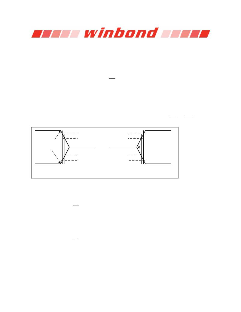
�VOH� -� x� mV�
�VOH� -� 2x� mV�
�tHZ�
�tRPST� end� point�
�VOL� +� 2x� mV�
�VOL� +� x� mV�
�T1� T2�
�tHZ,tRPST� end� point� =� 2� x� T1� -� T2�
�VTT� +� 2x� mV�
�VTT� +� x� mV�
�tLZ�
�tRPRE� begin� point�
�VTT� -� x� mV�
�VTT� -� 2x� mV�
�T1� T2�
�tLZ,tRPRE� begin� point� =� 2� x� T1� -� T2�
�Figure� 18�
�–� Method� for� calculating� transitions� and� endpoints�
�16.� Input� waveform� timing� tDS� with� differential� data� strobe� enabled� MR[bit10]=0.� There� are� two� sets� of� values� listed� for� DQ� and�
�DM� input� setup� time:� tDS(base)� and� tDS(ref).� The� tDS(ref)� value� (for� reference� only)� is� equivalent� to� the� baseline� value�
�tDS(base)� at� VREF� when� the� slew� rate� is� 2.0� V/nS,� differentially.� The� baseline� value� tDS(base)� is� the� JEDEC� defined� value,�
�referenced� from� the� input� signal� crossing� at� the� VIH(ac)� level� to� the� differential� data� strobe� crosspoint� for� a� rising� signal,� and�
�from� the� input� signal� crossing� at� the� VIL(ac)� level� to� the� differential� data� strobe� crosspoint� for� a� falling� signal� applied� to� the�
�device� under� test.� DQS,� DQS� signals� must� be� monotonic� between� VIL(dc)max� and� VIH(dc)min.� See� Figure� 19.� If� the�
�differential� DQS� slew� rate� is� not� equal� to� 2.0� V/nS,� then� the� baseline� values� must� be� derated� by� adding� the� values� from�
�table� of� DDR2-667,� DDR2-800� and� DDR2-1066� tDS/tDH� derating� with� differential� data� strobe� (page� 60).�
�17.� Input� waveform� timing� tDH� with� differential� data� strobe� enabled� MR[bit10]=0.� There� are� two� sets� of� values� listed� for� DQ� and�
�DM� input� hold� time:� tDH(base)� and� tDH(ref).� The� tDH(ref)� value� (for� reference� only)� is� equivalent� to� the� baseline� value�
�tDH(base)� at� VREF� when� the� slew� rate� is� 2.0� V/nS,� differentially.� The� baseline� value� tDH(base)� is� the� JEDEC� defined� value,�
�referenced� from� the� differential� data� strobe� crosspoint� to� the� input� signal� crossing� at� the� VIH(dc)� level� for� a� falling� signal� and�
�from� the� differential� data� strobe� crosspoint� to� the� input� signal� crossing� at� the� VIL(dc)� level� for� a� rising� signal� applied� to� the�
�device� under� test.� DQS,� DQS� signals� must� be� monotonic� between� VIL(dc)max� and� VIH(dc)min.� See� Figure� 19.� If� the�
�differential� DQS� slew� rate� is� not� equal� to� 2.0� V/nS,� then� the� baseline� values� must� be� derated� by� adding� the� values� from�
�table� of� DDR2-667,� DDR2-800� and� DDR2-1066� tDS/tDH� derating� with� differential� data� strobe� (page� 60).�
�Publication� Release� Date:� Nov.� 29,� 2011�
�-� 48� -�
�Revision� A02�
�相关PDF资料 |
PDF描述 |
|---|---|
| W9725G6KB-25I | IC DDR2 SDRAM 256MBIT 84WBGA |
| W972GG6JB-3I | IC DDR2 SDRAM 2GBITS 84WBGA |
| W9751G6IB-25 | IC DDR2-800 SDRAM 512MB 84-WBGA |
| W9751G6KB-25 | IC DDR2 SDRAM 512MBIT 84WBGA |
| W9812G6JH-6I | IC SDRAM 128MBIT 54TSOPII |
相关代理商/技术参数 |
参数描述 |
|---|---|
| W9725G6KB-18 | 制造商:Winbond Electronics 功能描述:IC MEMORY 制造商:Winbond Electronics Corp 功能描述:IC MEMORY |
| W9725G6KB-25 | 功能描述:IC DDR2 SDRAM 256MBIT 84WBGA RoHS:是 类别:集成电路 (IC) >> 存储器 系列:- 标准包装:1 系列:- 格式 - 存储器:闪存 存储器类型:闪存 - NAND 存储容量:4G(256M x 16) 速度:- 接口:并联 电源电压:2.7 V ~ 3.6 V 工作温度:0°C ~ 70°C 封装/外壳:48-TFSOP(0.724",18.40mm 宽) 供应商设备封装:48-TSOP I 包装:Digi-Reel® 其它名称:557-1461-6 |
| W9725G6KB-25 TR | 制造商:Winbond Electronics Corp 功能描述:256M DDR2-800, X16 |
| W9725G6KB25A | 制造商:WINBOND 制造商全称:Winbond 功能描述:DLL aligns DQ and DQS transitions with clock, Data masks (DM) for write data, Write Data Mask |
| W9725G6KB25I | 制造商:Winbond Electronics Corp 功能描述:DRAM Chip DDR2 SDRAM 256M-Bit 16Mx16 1.8V 84-Pin WBGA 制造商:Winbond Electronics 功能描述:IC DDR2 SDRAM 256M 2.5NS 84WBGA 制造商:Winbond Electronics Corp 功能描述:IC DDR2 SDRAM 256M 2.5NS 84WBGA 制造商:Winbond 功能描述:DRAM Chip DDR2 SDRAM 256M-Bit 16Mx16 1.8V 84-Pin WBGA |
发布紧急采购,3分钟左右您将得到回复。