- 您现在的位置:买卖IC网 > Datasheet目录369 > W9725G6JB25I (Winbond Electronics)IC DDR2 SDRAM 256MBIT 84WBGA Datasheet资料下载
参数资料
| 型号: | W9725G6JB25I |
| 厂商: | Winbond Electronics |
| 文件页数: | 66/87页 |
| 文件大小: | 0K |
| 描述: | IC DDR2 SDRAM 256MBIT 84WBGA |
| 标准包装: | 200 |
| 格式 - 存储器: | RAM |
| 存储器类型: | DDR2 SDRAM |
| 存储容量: | 256M(16Mx16) |
| 速度: | 2.5ns |
| 接口: | 并联 |
| 电源电压: | 1.7 V ~ 1.9 V |
| 工作温度: | -40°C ~ 95°C |
| 封装/外壳: | 84-TFBGA |
| 供应商设备封装: | 84-WBGA(8x12.5) |
| 包装: | 托盘 |
第1页第2页第3页第4页第5页第6页第7页第8页第9页第10页第11页第12页第13页第14页第15页第16页第17页第18页第19页第20页第21页第22页第23页第24页第25页第26页第27页第28页第29页第30页第31页第32页第33页第34页第35页第36页第37页第38页第39页第40页第41页第42页第43页第44页第45页第46页第47页第48页第49页第50页第51页第52页第53页第54页第55页第56页第57页第58页第59页第60页第61页第62页第63页第64页第65页当前第66页第67页第68页第69页第70页第71页第72页第73页第74页第75页第76页第77页第78页第79页第80页第81页第82页第83页第84页第85页第86页第87页
�� �
�
�W9725G6JB�
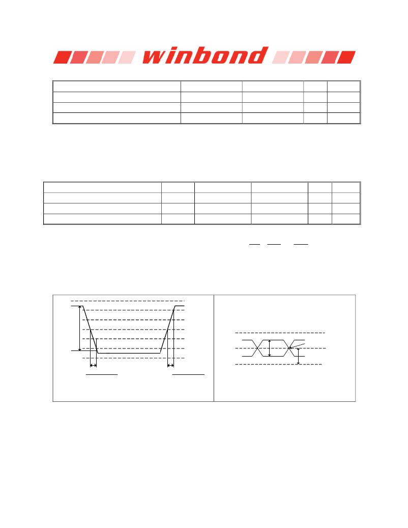
�9.12� AC� Input� Test� Conditions�
�CONDITION�
�Input� reference� voltage�
�Input� signal� maximum� peak� to� peak� swing�
�Input� signal� minimum� slew� rate�
�SYMBOL�
�V� REF�
�V� SWING(MAX)�
�SLEW�
�VALUE�
�0.5� x� V� DDQ�
�1.0�
�1.0�
�UNIT�
�V�
�V�
�V/nS�
�NOTES�
�1�
�1�
�2,� 3�
�Notes:�
�1.� Input� waveform� timing� is� referenced� to� the� input� signal� crossing� through� the� VIH/IL(ac)� level� applied� to� the� device� under� test.�
�2.� The� input� signal� minimum� slew� rate� is� to� be� maintained� over� the� range� from� VREF� to� VIH(ac)� min� for� rising� edges� and� the�
�range� from� VREF� to� VIL(ac)� max� for� falling� edges� as� shown� in� the� below� figure.�
�3.� AC� timings� are� referenced� with� input� waveforms� switching� from� VIL(ac)� to� VIH(ac)� on� the� positive� transitions� and� VIH(ac)� to�
�VIL(ac)� on� the� negative� transitions.�
�9.13� Differential� Input/Output� AC� Logic� Levels�
�PARAMETER�
�AC� differential� input� voltage�
�AC� differential� cross� point� input� voltage�
�AC� differential� cross� point� output� voltage�
�SYM.�
�V� ID� (ac)�
�V� IX� (ac)�
�V� OX� (ac)�
�MIN.�
�0.5�
�0.5� x� VDDQ� -� 0.175�
�0.5� x� VDDQ� -� 0.125�
�MAX.�
�VDDQ� +� 0.6�
�0.5� x� VDDQ� +� 0.175�
�0.5� x� VDDQ� +� 0.125�
�UNIT�
�V�
�V�
�V�
�NOTES�
�1�
�2�
�3�
�Notes:�
�1.� VID� (ac)� specifies� the� input� differential� voltage� |VTR� -VCP� |� required� for� switching,� where� VTR� is� the� true� input� signal� (such�
�as� CLK,� LDQS� or� UDQS)� and� VCP� is� the� complementary� input� signal� (such� as� CLK� ,� LDQS� or� UDQS� ).� The� minimum�
�value� is� equal� to� VIH� (ac)� -� VIL� (ac).�
�2.� The� typical� value� of� VIX� (ac)� is� expected� to� be� about� 0.5� x� VDDQ� of� the� transmitting� device� and� VIX� (ac)� is� expected� to� track�
�variations� in� VDDQ.� VIX� (ac)� indicates� the� voltage� at� which� differential� input� signals� must� cross.�
�3.� The� typical� value� of� VOX� (ac)� is� expected� to� be� about� 0.5� x� VDDQ� of� the� transmitting� device� and� VOX� (ac)� is� expected� to�
�track� variations� in� VDDQ.� VOX� (ac)� indicates� the� voltage� at� which� differential� output� signals� must� cross.�
�V� DDQ�
�V� IH(ac)� min�
�V� IH(dc)� min�
�V� SWING(MAX)�
�V� REF�
�V� IL(dc)� max�
�V� TR�
�V� DDQ�
�V� IL(ac)� max�
�V� SS�
�V� CP�
�V� ID�
�Crossing� point�
�V� IX� or� V� OX�
�Δ� TF�
�Δ� TR�
�V� SSQ�
�Falling� Slew� =�
�V� REF� -� V� IL(ac)� max�
�Δ� TF�
�Rising� Slew� =�
�V� IH(ac)� min� -� V� REF�
�Δ� TR�
�Figure� 28� –� AC� input� test� signal� and� Differential� signal� levels� waveform�
�Publication� Release� Date:� Nov.� 29,� 2011�
�-� 66� -�
�Revision� A02�
�相关PDF资料 |
PDF描述 |
|---|---|
| W9725G6KB-25I | IC DDR2 SDRAM 256MBIT 84WBGA |
| W972GG6JB-3I | IC DDR2 SDRAM 2GBITS 84WBGA |
| W9751G6IB-25 | IC DDR2-800 SDRAM 512MB 84-WBGA |
| W9751G6KB-25 | IC DDR2 SDRAM 512MBIT 84WBGA |
| W9812G6JH-6I | IC SDRAM 128MBIT 54TSOPII |
相关代理商/技术参数 |
参数描述 |
|---|---|
| W9725G6KB-18 | 制造商:Winbond Electronics 功能描述:IC MEMORY 制造商:Winbond Electronics Corp 功能描述:IC MEMORY |
| W9725G6KB-25 | 功能描述:IC DDR2 SDRAM 256MBIT 84WBGA RoHS:是 类别:集成电路 (IC) >> 存储器 系列:- 标准包装:1 系列:- 格式 - 存储器:闪存 存储器类型:闪存 - NAND 存储容量:4G(256M x 16) 速度:- 接口:并联 电源电压:2.7 V ~ 3.6 V 工作温度:0°C ~ 70°C 封装/外壳:48-TFSOP(0.724",18.40mm 宽) 供应商设备封装:48-TSOP I 包装:Digi-Reel® 其它名称:557-1461-6 |
| W9725G6KB-25 TR | 制造商:Winbond Electronics Corp 功能描述:256M DDR2-800, X16 |
| W9725G6KB25A | 制造商:WINBOND 制造商全称:Winbond 功能描述:DLL aligns DQ and DQS transitions with clock, Data masks (DM) for write data, Write Data Mask |
| W9725G6KB25I | 制造商:Winbond Electronics Corp 功能描述:DRAM Chip DDR2 SDRAM 256M-Bit 16Mx16 1.8V 84-Pin WBGA 制造商:Winbond Electronics 功能描述:IC DDR2 SDRAM 256M 2.5NS 84WBGA 制造商:Winbond Electronics Corp 功能描述:IC DDR2 SDRAM 256M 2.5NS 84WBGA 制造商:Winbond 功能描述:DRAM Chip DDR2 SDRAM 256M-Bit 16Mx16 1.8V 84-Pin WBGA |
发布紧急采购,3分钟左右您将得到回复。