参数资料
| 型号: | AD9557BCPZ |
| 厂商: | Analog Devices Inc |
| 文件页数: | 39/92页 |
| 文件大小: | 0K |
| 描述: | IC CLOCK TRANSLATOR 40LFCSP |
| 产品变化通告: | Minor Mask Change 11/Apr/2012 |
| 标准包装: | 1 |
| 类型: | 时钟/频率转换器 |
| PLL: | 是 |
| 主要目的: | 以太网,SONET/SDH |
| 输入: | CMOS,LVDS,LVPECL |
| 输出: | CMOS,HSTL,LVDS |
| 电路数: | 1 |
| 比率 - 输入:输出: | 2:2 |
| 差分 - 输入:输出: | 是/是 |
| 频率 - 最大: | 1.25GHz |
| 电源电压: | 1.71 V ~ 3.465 V |
| 工作温度: | -40°C ~ 85°C |
| 安装类型: | 表面贴装 |
| 封装/外壳: | 40-VFQFN 裸露焊盘,CSP |
| 供应商设备封装: | 40-LFCSP-VQ(6x6) |
| 包装: | 托盘 |
第1页第2页第3页第4页第5页第6页第7页第8页第9页第10页第11页第12页第13页第14页第15页第16页第17页第18页第19页第20页第21页第22页第23页第24页第25页第26页第27页第28页第29页第30页第31页第32页第33页第34页第35页第36页第37页第38页当前第39页第40页第41页第42页第43页第44页第45页第46页第47页第48页第49页第50页第51页第52页第53页第54页第55页第56页第57页第58页第59页第60页第61页第62页第63页第64页第65页第66页第67页第68页第69页第70页第71页第72页第73页第74页第75页第76页第77页第78页第79页第80页第81页第82页第83页第84页第85页第86页第87页第88页第89页第90页第91页第92页
AD9557
Data Sheet
Rev. B | Page 44 of 92
SERIAL CONTROL PORT
The AD9557 serial control port is a flexible, synchronous serial
communications port that provides a convenient interface to
many industry-standard microcontrollers and microprocessors.
The serial control port is compatible with most synchronous
transfer formats, including IC, Motorola SPI, and Intel SSR
protocols. The serial control port allows read/write access to the
AD9557 register map.
In SPI mode, single or multiple byte transfers are supported.
The SPI port configuration is programmable via Register 0x0000.
This register is integrated into the SPI control logic rather than
in the register map and is distinct from the I2C Register 0x0000.
It is also inaccessible to the EEPROM controller.
protocols, only one or the other is active following power-up
(as determined by the M0 and M1 multifunction pins during
the startup sequence). That is, the only way to change the serial
port protocol is to reset the device (or cycle the device power
supply).
SPI/IC PORT SELECTION
Because the AD9557 supports both SPI and IC protocols, the
active serial port protocol depends on the logic state of the
PINCONTROL, M1, and M0 pins. The PINCONTROL pin
must be low, and the state of the M0 and M1 pins determines
I2C address assignments.
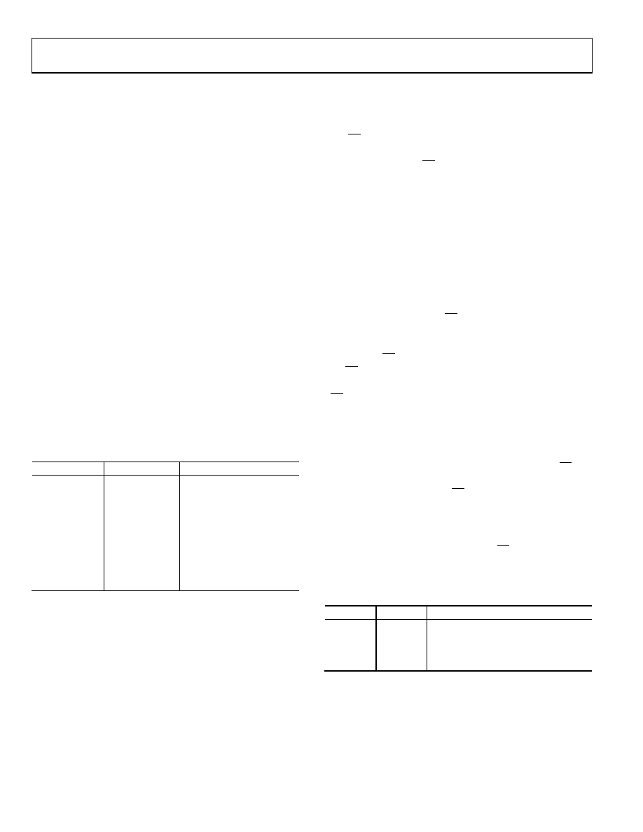
Table 24. SPI/IC Serial Port Setup
M1
M0
SPI/IC
Low
SPI
Low
Open
IC, 1101000
Low
High
IC, 1101001
Open
Low
IC, 1101010
Open
IC, 1101011
Open
High
IC, 1101100
High
Low
IC, 1101101
High
Open
IC, 1101110
High
IC, 1101111
SPI SERIAL PORT OPERATION
Pin Descriptions
The SCLK (serial clock) pin serves as the serial shift clock. This
pin is an input. SCLK synchronizes serial control port read and
write operations. The rising edge SCLK registers write data bits,
and the falling edge registers read data bits. The SCLK pin
supports a maximum clock rate of 40 MHz.
The SDIO (serial data input/output) pin is a dual-purpose pin
and acts as either an input only (unidirectional mode) or as both
an input and an output (bidirectional mode). The AD9557
default SPI mode is bidirectional.
The SDO (serial data output) pin is useful only in unidirectional
I/O mode. It serves as the data output pin for read operations.
The
EE
AA
(chip select) pin is an active low control that gates read
and write operations. This pin is internally connected to a 30 k
pull-up resistor. When
AA
CSEE
AA
is high, the SDO and SDIO pins go
into a high impedance state.
CS
SPI Mode Operation
The SPI port supports both 3-wire (bidirectional) and 4-wire
(unidirectional) hardware configurations and both MSB-first
and LSB-first data formats. Both the hardware configuration
and data format features are programmable. By default, the
AD9557 uses the bidirectional MSB-first mode. The reason that
bidirectional is the default mode is so that the user can still
write to the device, if it is wired for unidirectional operation, to
switch to unidirectional mode.
Assertion (active low) of the
AA
CSEE
AA
pin initiates a write or read
operation to the AD9557 SPI port. For data transfers of three
bytes or fewer (excluding the instruction word), the device
supports the
AA
CSEE
AA
stalled high mode (see Table 25). In this mode,
the
AA
CSEE
AA
pin can be temporarily deasserted on any byte boundary,
allowing time for the system controller to process the next byte.
AA
CSEE
AA
can be deasserted only on byte boundaries, however. This
applies to both the instruction and data portions of the transfer.
During stall high periods, the serial control port state machine
enters a wait state until all data is sent. If the system controller
decides to abort a transfer midstream, the state machine must be
reset either by completing the transfer or by asserting the
AA
CSEE
AA
pin for at least one complete SCLK cycle (but less than eight
SCLK cycles). Deasserting the
AA
CSEE
AA
pin on a nonbyte boundary
terminates the serial transfer and flushes the buffer.
In streaming mode (see Table 25), any number of data bytes can
be transferred in a continuous stream. The register address is
automatically incremented or decremented.
AA
CSEE
AA
must be deasserted
at the end of the last byte that is transferred, thereby ending the
stream mode.
Table 25. Byte Transfer Count
W1
W0
Bytes to Transfer
0
1
0
1
2
1
0
3
1
Streaming mode
相关PDF资料 |
PDF描述 |
|---|---|
| V375C36M150BG | CONVERTER MOD DC/DC 36V 150W |
| AD9547BCPZ | IC CLOCK GEN/SYNCHRONIZR 64LFCSP |
| D38999/20MF11JN | CONN RCPT 11POS WALL MNT W/SCKT |
| AD9549ABCPZ | IC CLOCK GEN/SYNCHRONIZR 64LFCSP |
| ADN2814ACPZ | IC CLOCK/DATA RECOVERY 32LFCSP |
相关代理商/技术参数 |
参数描述 |
|---|---|
| AD9557BCPZ-REEL7 | 功能描述:IC CLK XLATR PLL 1250MHZ 40LFCSP RoHS:是 类别:集成电路 (IC) >> 时钟/计时 - 专用 系列:- 标准包装:28 系列:- 类型:时钟/频率发生器 PLL:是 主要目的:Intel CPU 服务器 输入:时钟 输出:LVCMOS 电路数:1 比率 - 输入:输出:3:22 差分 - 输入:输出:无/是 频率 - 最大:400MHz 电源电压:3.135 V ~ 3.465 V 工作温度:0°C ~ 85°C 安装类型:表面贴装 封装/外壳:64-TFSOP (0.240",6.10mm 宽) 供应商设备封装:64-TSSOP 包装:管件 |
| AD9558 | 制造商:AD 制造商全称:Analog Devices 功能描述:Quad Input Multiservice Line Card Adaptive |
| AD9558/PCBZ | 功能描述:BOARD EVAL FOR AD9558 RoHS:是 类别:编程器,开发系统 >> 评估演示板和套件 系列:* 标准包装:1 系列:- 主要目的:电信,线路接口单元(LIU) 嵌入式:- 已用 IC / 零件:IDT82V2081 主要属性:T1/J1/E1 LIU 次要属性:- 已供物品:板,电源,线缆,CD 其它名称:82EBV2081 |
| AD9558BCPZ | 功能描述:IC CLOCK TRANSLATOR 64LFCSP RoHS:是 类别:集成电路 (IC) >> 时钟/计时 - 专用 系列:- 标准包装:1 系列:- 类型:时钟/频率发生器,多路复用器 PLL:是 主要目的:存储器,RDRAM 输入:晶体 输出:LVCMOS 电路数:1 比率 - 输入:输出:1:2 差分 - 输入:输出:无/是 频率 - 最大:400MHz 电源电压:3 V ~ 3.6 V 工作温度:0°C ~ 85°C 安装类型:表面贴装 封装/外壳:16-TSSOP(0.173",4.40mm 宽) 供应商设备封装:16-TSSOP 包装:Digi-Reel® 其它名称:296-6719-6 |
| AD9558BCPZ-REEL7 | 功能描述:IC CLK XLATR PLL 1250MHZ 64LFCSP RoHS:是 类别:集成电路 (IC) >> 时钟/计时 - 专用 系列:- 标准包装:28 系列:- 类型:时钟/频率发生器 PLL:是 主要目的:Intel CPU 服务器 输入:时钟 输出:LVCMOS 电路数:1 比率 - 输入:输出:3:22 差分 - 输入:输出:无/是 频率 - 最大:400MHz 电源电压:3.135 V ~ 3.465 V 工作温度:0°C ~ 85°C 安装类型:表面贴装 封装/外壳:64-TFSOP (0.240",6.10mm 宽) 供应商设备封装:64-TSSOP 包装:管件 |
发布紧急采购,3分钟左右您将得到回复。