参数资料
| 型号: | AD9557BCPZ |
| 厂商: | Analog Devices Inc |
| 文件页数: | 86/92页 |
| 文件大小: | 0K |
| 描述: | IC CLOCK TRANSLATOR 40LFCSP |
| 产品变化通告: | Minor Mask Change 11/Apr/2012 |
| 标准包装: | 1 |
| 类型: | 时钟/频率转换器 |
| PLL: | 是 |
| 主要目的: | 以太网,SONET/SDH |
| 输入: | CMOS,LVDS,LVPECL |
| 输出: | CMOS,HSTL,LVDS |
| 电路数: | 1 |
| 比率 - 输入:输出: | 2:2 |
| 差分 - 输入:输出: | 是/是 |
| 频率 - 最大: | 1.25GHz |
| 电源电压: | 1.71 V ~ 3.465 V |
| 工作温度: | -40°C ~ 85°C |
| 安装类型: | 表面贴装 |
| 封装/外壳: | 40-VFQFN 裸露焊盘,CSP |
| 供应商设备封装: | 40-LFCSP-VQ(6x6) |
| 包装: | 托盘 |
第1页第2页第3页第4页第5页第6页第7页第8页第9页第10页第11页第12页第13页第14页第15页第16页第17页第18页第19页第20页第21页第22页第23页第24页第25页第26页第27页第28页第29页第30页第31页第32页第33页第34页第35页第36页第37页第38页第39页第40页第41页第42页第43页第44页第45页第46页第47页第48页第49页第50页第51页第52页第53页第54页第55页第56页第57页第58页第59页第60页第61页第62页第63页第64页第65页第66页第67页第68页第69页第70页第71页第72页第73页第74页第75页第76页第77页第78页第79页第80页第81页第82页第83页第84页第85页当前第86页第87页第88页第89页第90页第91页第92页
Data Sheet
AD9557
Rev. B | Page 87 of 92
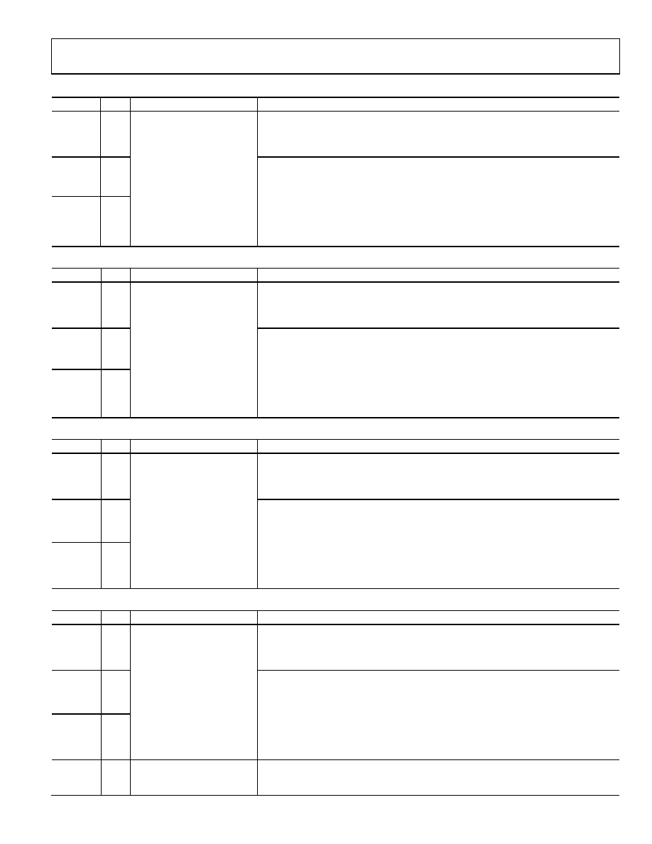
Table 112. EEPROM Storage Sequence for General Configuration Settings
Address
Bits
Bit Name
Description
0x0E17
[7:0]
General
The default value of this register is 0x11, which the controller interprets as a data
instruction. Its decimal value is 17, so this tells the controller to transfer 18 bytes of data
(17 + 1), beginning at the address specified by the next two bytes. The controller stores
0x11 in the EEPROM and increments the EEPROM address pointer.
0x0E18
[7:0]
The default value of these two registers is 0x0200. Note that Register 0x0E18 and
Register 0x0E19 are the most significant and least significant bytes of the target address,
respectively. Because the previous register contains a data instruction, these two
registers define a starting address (in this case, 0x0200). The controller stores 0x0200 in
the EEPROM and increments the EEPROM pointer by 2. It then transfers 18 bytes from
the register map (beginning at Address 0x0200) to the EEPROM and increments the
EEPROM address pointer by 19 (18 data bytes and one checksum byte). The 18 bytes
transferred correspond to the general configuration parameters in the register map.
0x0E19
[7:0]
Table 113. EEPROM Storage Sequence for DPLL Settings
Address
Bits
Bit Name
Description
0x0E1A
[7:0]
DPLL
The default value of this register is 0x2E, which the controller interprets as a data
instruction. Its decimal value is 46, so this tells the controller to transfer 47 bytes of data
(46 + 1), beginning at the address specified by the next two bytes. The controller stores
0x2E in the EEPROM and increments the EEPROM address pointer.
0x0E1B
[7:0]
The default value of these two registers is 0x03. Note that Register 0x0E1B and
Register 0x0E1C are the most significant and least significant bytes of the target address,
respectively. Because the previous register contains a data instruction, these two
registers define a starting address (in this case, 0x0300). The controller stores 0x0300 in
the EEPROM and increments the EEPROM pointer by 2. It then transfers 47 bytes from
the register map (beginning at Address 0x0300) to the EEPROM and increments the
EEPROM address pointer by 48 (47 data bytes and one checksum byte). The 47 bytes
transferred correspond to the DPLL parameters in the register map.
0x0E1C
[7:0]
Table 114. EEPROM Storage Sequence for APLL Settings
Address
Bits
Bit Name
Description
0x0E1D
[7:0]
APLL
The default value of this register is 0x08, which the controller interprets as a data instruction.
Its decimal value is 8, so this tells the controller to transfer nine bytes of data (8 + 1),
beginning at the address specified by the next two bytes. The controller stores 0x08 in
the EEPROM and increments the EEPROM address pointer.
0x0E1E
[7:0]
The default value of these two registers is 0x0400. Note that Register 0x0E1E and
Register 0x0E1F are the most significant and least significant bytes of the target address,
respectively. Because the previous register contains a data instruction, these two registers
define a starting address (in this case, 0x0400). The controller stores 0x0400 in the EEPROM
and increments the EEPROM pointer by 2. It then transfers nine bytes from the register
map (beginning at Address 0x0400) to the EEPROM and increments the EEPROM address
pointer by 10 (nine data bytes and one checksum byte). The nine bytes transferred
correspond to APLL parameters in the register map.
0x0E1F
[7:0]
Table 115. EEPROM Storage Sequence for Clock Distribution Settings
Address
Bits
Bit Name
Description
0x0E20
[7:0]
Clock distribution
The default value of this register is 0x15, which the controller interprets as a data instruction.
Its decimal value is 21, so this tells the controller to transfer 22 bytes of data (21+1),
beginning at the address specified by the next two bytes. The controller stores 0x15 in
the EEPROM and increments the EEPROM address pointer.
0x0E21
[7:0]
The default value of these two registers is 0x0500. Note that Register 0x0E21 and
Register 0x0E22 are the most significant and least significant bytes of the target address,
respectively. Because the previous register contains a data instruction, these two registers
define a starting address (in this case, 0x0500). The controller stores 0x0500 in the EEPROM
and increments the EEPROM pointer by 2. It then transfers 22 bytes from the register map
(beginning at Address 0x0500) to the EEPROM and increments the EEPROM address
pointer by 23 (22 data bytes and one checksum byte). The 22 bytes transferred correspond to
the clock distribution parameters in the register map.
0x0E22
[7:0]
0x0E23
[7:0]
I/O update
The default value of this register is 0x80, which the controller interprets as an I/O update
instruction. The controller stores 0x80 in the EEPROM and increments the EEPROM address
pointer.
相关PDF资料 |
PDF描述 |
|---|---|
| V375C36M150BG | CONVERTER MOD DC/DC 36V 150W |
| AD9547BCPZ | IC CLOCK GEN/SYNCHRONIZR 64LFCSP |
| D38999/20MF11JN | CONN RCPT 11POS WALL MNT W/SCKT |
| AD9549ABCPZ | IC CLOCK GEN/SYNCHRONIZR 64LFCSP |
| ADN2814ACPZ | IC CLOCK/DATA RECOVERY 32LFCSP |
相关代理商/技术参数 |
参数描述 |
|---|---|
| AD9557BCPZ-REEL7 | 功能描述:IC CLK XLATR PLL 1250MHZ 40LFCSP RoHS:是 类别:集成电路 (IC) >> 时钟/计时 - 专用 系列:- 标准包装:28 系列:- 类型:时钟/频率发生器 PLL:是 主要目的:Intel CPU 服务器 输入:时钟 输出:LVCMOS 电路数:1 比率 - 输入:输出:3:22 差分 - 输入:输出:无/是 频率 - 最大:400MHz 电源电压:3.135 V ~ 3.465 V 工作温度:0°C ~ 85°C 安装类型:表面贴装 封装/外壳:64-TFSOP (0.240",6.10mm 宽) 供应商设备封装:64-TSSOP 包装:管件 |
| AD9558 | 制造商:AD 制造商全称:Analog Devices 功能描述:Quad Input Multiservice Line Card Adaptive |
| AD9558/PCBZ | 功能描述:BOARD EVAL FOR AD9558 RoHS:是 类别:编程器,开发系统 >> 评估演示板和套件 系列:* 标准包装:1 系列:- 主要目的:电信,线路接口单元(LIU) 嵌入式:- 已用 IC / 零件:IDT82V2081 主要属性:T1/J1/E1 LIU 次要属性:- 已供物品:板,电源,线缆,CD 其它名称:82EBV2081 |
| AD9558BCPZ | 功能描述:IC CLOCK TRANSLATOR 64LFCSP RoHS:是 类别:集成电路 (IC) >> 时钟/计时 - 专用 系列:- 标准包装:1 系列:- 类型:时钟/频率发生器,多路复用器 PLL:是 主要目的:存储器,RDRAM 输入:晶体 输出:LVCMOS 电路数:1 比率 - 输入:输出:1:2 差分 - 输入:输出:无/是 频率 - 最大:400MHz 电源电压:3 V ~ 3.6 V 工作温度:0°C ~ 85°C 安装类型:表面贴装 封装/外壳:16-TSSOP(0.173",4.40mm 宽) 供应商设备封装:16-TSSOP 包装:Digi-Reel® 其它名称:296-6719-6 |
| AD9558BCPZ-REEL7 | 功能描述:IC CLK XLATR PLL 1250MHZ 64LFCSP RoHS:是 类别:集成电路 (IC) >> 时钟/计时 - 专用 系列:- 标准包装:28 系列:- 类型:时钟/频率发生器 PLL:是 主要目的:Intel CPU 服务器 输入:时钟 输出:LVCMOS 电路数:1 比率 - 输入:输出:3:22 差分 - 输入:输出:无/是 频率 - 最大:400MHz 电源电压:3.135 V ~ 3.465 V 工作温度:0°C ~ 85°C 安装类型:表面贴装 封装/外壳:64-TFSOP (0.240",6.10mm 宽) 供应商设备封装:64-TSSOP 包装:管件 |
发布紧急采购,3分钟左右您将得到回复。