- 您现在的位置:买卖IC网 > PDF目录4591 > DS34T108GN+ (Maxim Integrated Products)IC TDM OVER PACKET 484HSBGA PDF资料下载
参数资料
| 型号: | DS34T108GN+ |
| 厂商: | Maxim Integrated Products |
| 文件页数: | 307/366页 |
| 文件大小: | 0K |
| 描述: | IC TDM OVER PACKET 484HSBGA |
| 产品培训模块: | Lead (SnPb) Finish for COTS Obsolescence Mitigation Program |
| 标准包装: | 30 |
| 类型: | TDM(分时复用) |
| 应用: | 数据传输 |
| 安装类型: | 表面贴装 |
| 封装/外壳: | 484-BGA 裸露焊盘 |
| 供应商设备封装: | 484-HSBGA(23x23) |
| 包装: | 托盘 |
| 产品目录页面: | 1429 (CN2011-ZH PDF) |
第1页第2页第3页第4页第5页第6页第7页第8页第9页第10页第11页第12页第13页第14页第15页第16页第17页第18页第19页第20页第21页第22页第23页第24页第25页第26页第27页第28页第29页第30页第31页第32页第33页第34页第35页第36页第37页第38页第39页第40页第41页第42页第43页第44页第45页第46页第47页第48页第49页第50页第51页第52页第53页第54页第55页第56页第57页第58页第59页第60页第61页第62页第63页第64页第65页第66页第67页第68页第69页第70页第71页第72页第73页第74页第75页第76页第77页第78页第79页第80页第81页第82页第83页第84页第85页第86页第87页第88页第89页第90页第91页第92页第93页第94页第95页第96页第97页第98页第99页第100页第101页第102页第103页第104页第105页第106页第107页第108页第109页第110页第111页第112页第113页第114页第115页第116页第117页第118页第119页第120页第121页第122页第123页第124页第125页第126页第127页第128页第129页第130页第131页第132页第133页第134页第135页第136页第137页第138页第139页第140页第141页第142页第143页第144页第145页第146页第147页第148页第149页第150页第151页第152页第153页第154页第155页第156页第157页第158页第159页第160页第161页第162页第163页第164页第165页第166页第167页第168页第169页第170页第171页第172页第173页第174页第175页第176页第177页第178页第179页第180页第181页第182页第183页第184页第185页第186页第187页第188页第189页第190页第191页第192页第193页第194页第195页第196页第197页第198页第199页第200页第201页第202页第203页第204页第205页第206页第207页第208页第209页第210页第211页第212页第213页第214页第215页第216页第217页第218页第219页第220页第221页第222页第223页第224页第225页第226页第227页第228页第229页第230页第231页第232页第233页第234页第235页第236页第237页第238页第239页第240页第241页第242页第243页第244页第245页第246页第247页第248页第249页第250页第251页第252页第253页第254页第255页第256页第257页第258页第259页第260页第261页第262页第263页第264页第265页第266页第267页第268页第269页第270页第271页第272页第273页第274页第275页第276页第277页第278页第279页第280页第281页第282页第283页第284页第285页第286页第287页第288页第289页第290页第291页第292页第293页第294页第295页第296页第297页第298页第299页第300页第301页第302页第303页第304页第305页第306页当前第307页第308页第309页第310页第311页第312页第313页第314页第315页第316页第317页第318页第319页第320页第321页第322页第323页第324页第325页第326页第327页第328页第329页第330页第331页第332页第333页第334页第335页第336页第337页第338页第339页第340页第341页第342页第343页第344页第345页第346页第347页第348页第349页第350页第351页第352页第353页第354页第355页第356页第357页第358页第359页第360页第361页第362页第363页第364页第365页第366页
____________________________________________________ DS34T101, DS34T102, DS34T104, DS34T108
45 of 366
Table 10-1. CPU Data Bus Widths
Value
Data Bus
Width
Access to
Chip Internal
Resources
Access to
SDRAM
Data Bus
Bits
MSB
Pins Used
1
32 bits
32 bit only
8, 16, 32 bit
H_D[31:0]
H_D[31]
3:0
0
16 bits
16 bit only
8, 16 bit
H_D[15:0]
H_D[15]
1:0
Burst accesses are not supported. The device uses the big-endian byte order, as explained in section 11.1.
The CPU starts an access to the device by asserting the H_CS_N signal (active low), accompanied by the desired
read/write state on H_R_W_N, address on H_AD[24:1], write byte enables on the H_WR_BE pins and valid data
(for a write access) on the H_D[31:0] pins. In response, the device asserts H_READY_N to indicate that the access
has been carried out. The ready assertion indicates that data from the CPU has been written into the device
register or external SDRAM (for write access) or that valid data from register/SDRAM is present on the data bus
(for read access). In response to H_READY_N assertion, the CPU de-asserts H_CS_N. This causes the chip to
de-assert H_READY_N, and thereby finish the CPU access.
In order to make CPU operation more efficient, the device immediately asserts H_READY_N during a write access.
On successive accesses (write or read) H_READY_N is asserted only after the previous write has been completed.
In 32-bit bus mode, H_WR_BE0_N through H_WR_BE3_N serve as write byte enable signals, replacing the
functionality of H_AD[1:0] in the address bus. In 16-bit bus mode, H_WR_BE0_N and H_WR_BE1_N serve as
write byte enables, replacing the functionality of H_AD[0] in the address bus. These signals enable byte-resolution
write access to the external SDRAM.
When performing a write access to internal chip resources, all H_WR_BE pins should be asserted since write
access to device registers must be done at the full bus width only.
Examples of read and write accesses on 32- and 16-bit buses are shown in the figures below.
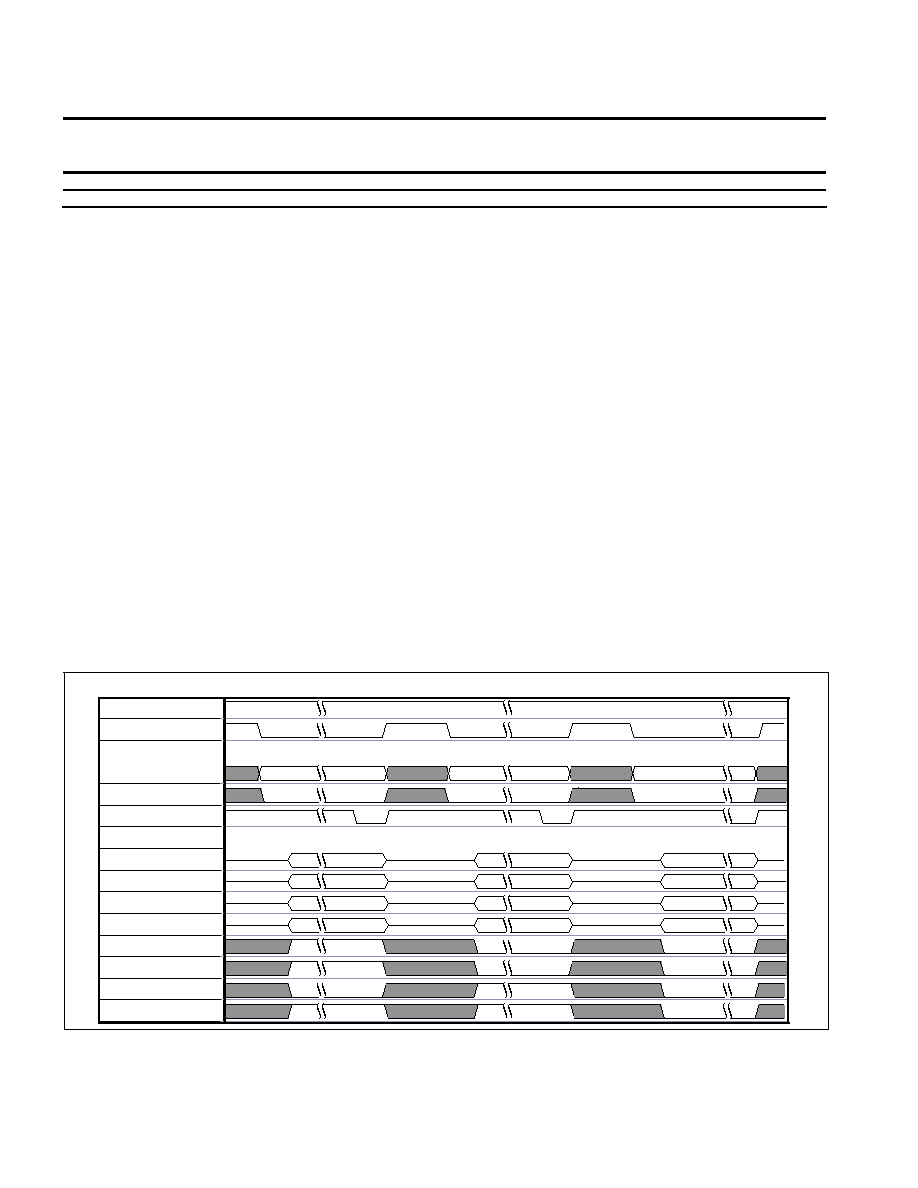
Figure 10-2. Write Access, 32-Bit Bus
DAT_32_16_N[0]
H_CS_N[0]
H_AD[24:1]
H_R_W_N[0]
H_READY_N[0]
[0]
H_D[31:24]
H_D[23:16]
H_D[15:8]
H_D[7:0]
H_WR_BE3_N[0]
H_WR_BE2_N[0]
H_WR_BE1_N[0]
H_WR_BE0_N[0]
cpu_addr[[1]='don't care'
cpu_addr[1]='don't care'
data ignored
valid
data ignored
valid
data ignored
valid
data_ignored
data ignored
valid
SDRAM WRITE ACCESS
32 bit data bus
INTERNAL
Figure 10-2 shows two write accesses to the SDRAM, one to a byte (at address 2) and the other to a word (at
addresses 0 and 1), followed by a write access to the internal chip resources.
相关PDF资料 |
PDF描述 |
|---|---|
| DS34T104GN+ | IC TDM OVER PACKET 484TEBGA |
| DS34T101GN+ | IC TDM OVER PACKET 484TEBGA |
| MIC2211-GOYML TR | IC REG LDO 1.8V/2.9V 10-MLF |
| MIC2211-GJYML TR | IC REG LDO 1.8V/2.5V 10-MLF |
| MIC2211-SGYML TR | IC REG LDO 3.3V/1.8V 10-MLF |
相关代理商/技术参数 |
参数描述 |
|---|---|
| DS34T108GN+ | 功能描述:以太网 IC Octal TDM Over Packet Chip RoHS:否 制造商:Micrel 产品:Ethernet Switches 收发器数量:2 数据速率:10 Mb/s, 100 Mb/s 电源电压-最大:1.25 V, 3.45 V 电源电压-最小:1.15 V, 3.15 V 最大工作温度:+ 85 C 封装 / 箱体:QFN-64 封装:Tray |
| DS35 | 制造商:LUMILEDS 制造商全称:LUMILEDS 功能描述:power light source Luxeon Dental |
| DS3500N+ | 制造商:Maxim Integrated Products 功能描述:- Rail/Tube |
| DS3500N+T&R | 制造商:Maxim Integrated Products 功能描述:- Tape and Reel |
| DS3501 | 制造商:MAXIM 制造商全称:Maxim Integrated Products 功能描述:High-Voltage, NV, I2C POT with Temp Sensor and Lookup Table |
发布紧急采购,3分钟左右您将得到回复。