- 您现在的位置:买卖IC网 > PDF目录67681 > IBM21P100BGB PCI BUS CONTROLLER, PBGA304 PDF资料下载
参数资料
| 型号: | IBM21P100BGB |
| 元件分类: | 总线控制器 |
| 英文描述: | PCI BUS CONTROLLER, PBGA304 |
| 封装: | 31 X 31 MM, HEAT SINK, PLASTIC, BGA-304 |
| 文件页数: | 89/140页 |
| 文件大小: | 2032K |
| 代理商: | IBM21P100BGB |
第1页第2页第3页第4页第5页第6页第7页第8页第9页第10页第11页第12页第13页第14页第15页第16页第17页第18页第19页第20页第21页第22页第23页第24页第25页第26页第27页第28页第29页第30页第31页第32页第33页第34页第35页第36页第37页第38页第39页第40页第41页第42页第43页第44页第45页第46页第47页第48页第49页第50页第51页第52页第53页第54页第55页第56页第57页第58页第59页第60页第61页第62页第63页第64页第65页第66页第67页第68页第69页第70页第71页第72页第73页第74页第75页第76页第77页第78页第79页第80页第81页第82页第83页第84页第85页第86页第87页第88页当前第89页第90页第91页第92页第93页第94页第95页第96页第97页第98页第99页第100页第101页第102页第103页第104页第105页第106页第107页第108页第109页第110页第111页第112页第113页第114页第115页第116页第117页第118页第119页第120页第121页第122页第123页第124页第125页第126页第127页第128页第129页第130页第131页第132页第133页第134页第135页第136页第137页第138页第139页第140页
IBM21P100BGB
IBM 133 PCI-X Bridge R1.1
Configuration Registers
Page 44 of 131
ppb11_pcix_regs.fm.03
July 9, 2001
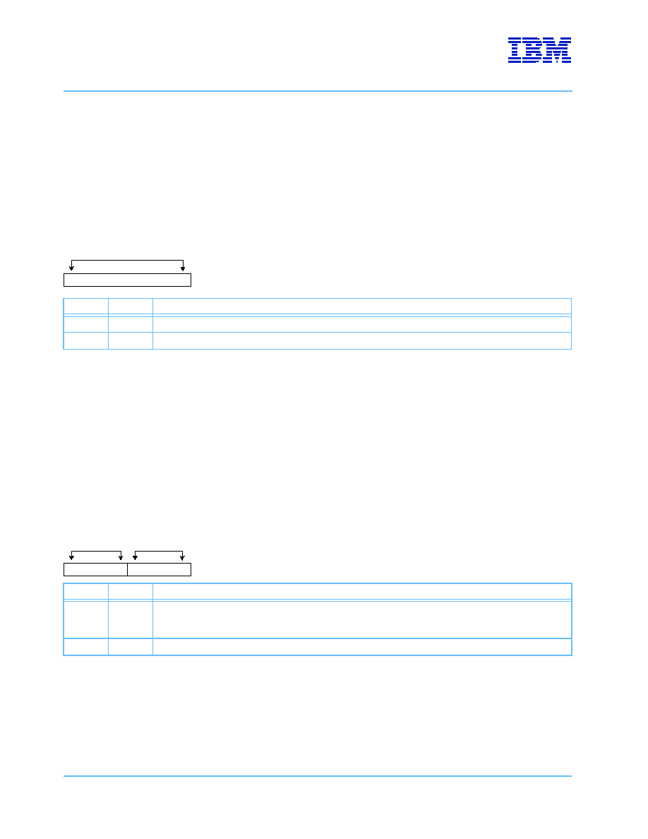
5.2.4.15 Secondary Latency Timer Register
This register specifies, in PCI bus clock units, the value of the Secondary Latency Timer for this device as a
bus master. Masters that can burst for more than two data phases must implement this register as Read/
Write.
5.2.4.16 I/O Base Register
The I/O Base register specifies the base of the I/O address range bits 15:12 and is used in conjunction with
the I/O Limit register and I/O Base Upper 16 Bits and I/O Limit Upper 16 Bits registers to specify a range of
32-bit addresses supported for I/O transactions on the PCI Bus. Address bits 11:0 are assumed to be x‘000’
for the base address. This register also specifies that the bridge supports 32-bit I/O addressing.
Address Offset
x‘1B’
Access
See individual fields
Reset Value
x'00' in PCI mode, x'40' in PCI-X mode
Secondary Latency Timer
7654
3210
Bit(s)
Access
Field Name and Description
7:3
RW
Read/Write to set granularity in 8-cycle increments.
2:0
RO
Forced to b‘000’ to force 8-cycle increments for the latency timer.
Address Offset
x‘1C’
Access
See individual fields
Reset Value
x‘X1’
I/O Base
Address
32-Bit
Addressing
7654
3210
Bit(s)
Access
Field Name and Description
7:4
RW
I/O Base Address
Address bits 15:12 of the base address for the address range of I/O operations that are passed from the primary
to the secondary PCI bus.
3:0
RO
Set to b‘0001’ to indicate that 32-bit I/O addressing is supported.
相关PDF资料 |
PDF描述 |
|---|---|
| IBM21P100BGC | PCI BUS CONTROLLER, PBGA304 |
| IBM25403GCX-3JC76C2 | RISC PROCESSOR, PQFP16 |
| IBM25405GP-3BA200C2 | RISC PROCESSOR, PBGA456 |
| IBM25EMPPC603EFG-100 | 32-BIT, 100 MHz, RISC PROCESSOR, PQFP240 |
| IBM25EMPPC603EBG-100 | 32-BIT, 100 MHz, RISC PROCESSOR, CBGA255 |
相关代理商/技术参数 |
参数描述 |
|---|---|
| IBM24L5086 | 制造商:AVED MEMORY PRODUCTS 功能描述: 制造商:AVED Memory Products 功能描述: |
| IBM25403GCX-3BC80C2 | 制造商:IBM 功能描述:RISC PROCESSOR, 160 Pin Plastic BGA |
| IBM25403GCX-3JC50C2 | 制造商:IBM 功能描述:403GCX-3JC50C2 |
| IBM25403GCX-3JC66C2 | 制造商:IBM 功能描述: |
| IBM25403GCX3JC76C2 | 制造商:IBM 功能描述: |
发布紧急采购,3分钟左右您将得到回复。