- 您现在的位置:买卖IC网 > PDF目录296408 > M58WR064KU70ZA6U (NUMONYX) 4M X 16 FLASH 1.8V PROM, 70 ns, PBGA44 PDF资料下载
参数资料
| 型号: | M58WR064KU70ZA6U |
| 厂商: | NUMONYX |
| 元件分类: | PROM |
| 英文描述: | 4M X 16 FLASH 1.8V PROM, 70 ns, PBGA44 |
| 封装: | 7.50 X 5 MM, 0.50 MM PITCH, ROHS COMPLIANT, VFBGA-44 |
| 文件页数: | 5/122页 |
| 文件大小: | 2187K |
| 代理商: | M58WR064KU70ZA6U |
第1页第2页第3页第4页当前第5页第6页第7页第8页第9页第10页第11页第12页第13页第14页第15页第16页第17页第18页第19页第20页第21页第22页第23页第24页第25页第26页第27页第28页第29页第30页第31页第32页第33页第34页第35页第36页第37页第38页第39页第40页第41页第42页第43页第44页第45页第46页第47页第48页第49页第50页第51页第52页第53页第54页第55页第56页第57页第58页第59页第60页第61页第62页第63页第64页第65页第66页第67页第68页第69页第70页第71页第72页第73页第74页第75页第76页第77页第78页第79页第80页第81页第82页第83页第84页第85页第86页第87页第88页第89页第90页第91页第92页第93页第94页第95页第96页第97页第98页第99页第100页第101页第102页第103页第104页第105页第106页第107页第108页第109页第110页第111页第112页第113页第114页第115页第116页第117页第118页第119页第120页第121页第122页
Common flash interface
M58WRxxxKU, M58WRxxxKL
102/123
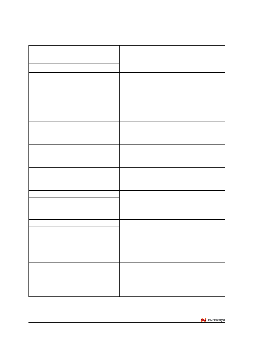
Table 46.
Bank and erase block region 2 information(1)
M58WR016KU,
M58WR032KU,
M58WR064KU
M58WR016KL,
M58WR032KL,
M58WR064KL
Description
Offset
Data
Offset
Data
(P+28)h = 61h
01h
(P+30)h = 69h
03h(2)
07h(3)
0Fh(4)
Number of identical banks within Bank Region 2
(P+29)h = 62h
00h
(P+31)h = 6Ah
00h
(P+2A)h = 63h
11h
(P+32)h = 6Bh
11h
Number of program or erase operations allowed in Bank
Region 2:
Bits 0-3: number of simultaneous program operations
Bits 4-7: number of simultaneous erase operations
(P+2B)h = 64h
00h
(P+33)h = 6Ch
00h
Number of program or erase operations allowed in other
banks while a bank in this region is programming
Bits 0-3: number of simultaneous program operations
Bits 4-7: number of simultaneous erase operations
(P+2C)h = 65h
00h
(P+34)h = 6Dh
00h
Number of program or erase operations allowed in other
banks while a bank in this region is erasing
Bits 0-3: number of simultaneous program operations
Bits 4-7: number of simultaneous erase operations
(P+2D)h = 66h
02h
(P+35)h = 6Eh
01h
Types of erase block regions in Bank Region 2
n = number of erase block regions with contiguous same-
size erase blocks.
Symmetrically blocked banks have one blocking region.(5)
(P+2E)h = 67h
06h
(P+36)h = 6Fh
07h
Bank Region 2 Erase Block Type 1 Information
Bits 0-15: n+1 = number of identical-sized erase blocks
Bits 16-31: n×256 = number of bytes in erase block region
(P+2F)h = 68h
00h
(P+37)h = 70h
00h
(P+30)h = 69h
00h
(P+38)h = 71h
00h
(P+31)h = 6Ah
01h
(P+39)h = 72h
01h
(P+32)h = 6Bh
64h
(P+3A)h = 73h
64h
Bank Region 2 (Erase Block Type 1)
Minimum block erase cycles × 1000
(P+33)h = 6Ch
00h
(P+3B)h = 74h
00h
(P+34)h = 6Dh
01h
(P+3C)h = 75h
01h
Bank Region 2 (Erase Block Type 1): bits per cell, internal
ECC
Bits 0-3: bits per cell in erase region
Bit 4: reserved for “internal ECC used”
Bits 5-7: reserved
(P+35)h = 6Eh
03h
(P+3D)h = 76h
03h
Bank Region 2 (Erase Block Type 1): Page mode and
synchronous mode capabilities (defined in Table 43)
Bit 0: page-mode reads permitted
Bit 1: synchronous reads permitted
Bit 2: synchronous writes permitted
Bits 3-7: reserved
相关PDF资料 |
PDF描述 |
|---|---|
| M5L28FGNFREQ | CRYSTAL OSCILLATOR, CLOCK, 1.544 MHz - 125 MHz, HCMOS OUTPUT |
| M3L13TCNFREQ | CRYSTAL OSCILLATOR, CLOCK, 1.544 MHz - 125 MHz, HCMOS OUTPUT |
| M3L14FCNFREQ | CRYSTAL OSCILLATOR, CLOCK, 1.544 MHz - 125 MHz, HCMOS OUTPUT |
| M3L15TGNFREQ | CRYSTAL OSCILLATOR, CLOCK, 1.544 MHz - 125 MHz, HCMOS OUTPUT |
| M5L13TCNFREQ | CRYSTAL OSCILLATOR, CLOCK, 1.544 MHz - 125 MHz, HCMOS OUTPUT |
相关代理商/技术参数 |
参数描述 |
|---|---|
| M58WR064T | 制造商:STMICROELECTRONICS 制造商全称:STMicroelectronics 功能描述:64 Mbit (4Mb x 16, Multiple Bank, Burst ) 1.8V Supply Flash Memory |
| M58WR064T100ZB6T | 制造商:STMICROELECTRONICS 制造商全称:STMicroelectronics 功能描述:64 Mbit (4Mb x 16, Multiple Bank, Burst ) 1.8V Supply Flash Memory |
| M58WR064T70ZB6T | 制造商:STMICROELECTRONICS 制造商全称:STMicroelectronics 功能描述:64 Mbit (4Mb x 16, Multiple Bank, Burst ) 1.8V Supply Flash Memory |
| M58WR064T85ZB6T | 制造商:STMICROELECTRONICS 制造商全称:STMicroelectronics 功能描述:64 Mbit (4Mb x 16, Multiple Bank, Burst ) 1.8V Supply Flash Memory |
| M58WR128EB | 制造商:STMICROELECTRONICS 制造商全称:STMicroelectronics 功能描述:128 Mbit 8Mb x 16, Multiple Bank, Burst 1.8V Supply Flash Memory |
发布紧急采购,3分钟左右您将得到回复。