- 您现在的位置:买卖IC网 > PDF目录18765 > MRF89XAT-I/MQ (Microchip Technology)RF ISM BAND TXRX 32 QFN PDF资料下载
参数资料
| 型号: | MRF89XAT-I/MQ |
| 厂商: | Microchip Technology |
| 文件页数: | 14/140页 |
| 文件大小: | 0K |
| 描述: | RF ISM BAND TXRX 32 QFN |
| 标准包装: | 1 |
| 频率: | 863MHz ~ 870MHz,902MHz ~ 928MHz,950MHz ~ 960MHz |
| 数据传输率 - 最大: | 200kbps |
| 调制或协议: | FSK,OOK |
| 应用: | ISM |
| 功率 - 输出: | 12.5dBm |
| 灵敏度: | -113dBm |
| 电源电压: | 2.1 V ~ 3.6 V |
| 电流 - 接收: | 3mA |
| 电流 - 传输: | 25mA |
| 数据接口: | PCB,表面贴装 |
| 存储容量: | * |
| 天线连接器: | PCB,表面贴装 |
| 工作温度: | -40°C ~ 85°C |
| 封装/外壳: | 32-WFQFN 裸露焊盘 |
| 包装: | 标准包装 |
| 其它名称: | MRF89XAT-I/MQDKR |
第1页第2页第3页第4页第5页第6页第7页第8页第9页第10页第11页第12页第13页当前第14页第15页第16页第17页第18页第19页第20页第21页第22页第23页第24页第25页第26页第27页第28页第29页第30页第31页第32页第33页第34页第35页第36页第37页第38页第39页第40页第41页第42页第43页第44页第45页第46页第47页第48页第49页第50页第51页第52页第53页第54页第55页第56页第57页第58页第59页第60页第61页第62页第63页第64页第65页第66页第67页第68页第69页第70页第71页第72页第73页第74页第75页第76页第77页第78页第79页第80页第81页第82页第83页第84页第85页第86页第87页第88页第89页第90页第91页第92页第93页第94页第95页第96页第97页第98页第99页第100页第101页第102页第103页第104页第105页第106页第107页第108页第109页第110页第111页第112页第113页第114页第115页第116页第117页第118页第119页第120页第121页第122页第123页第124页第125页第126页第127页第128页第129页第130页第131页第132页第133页第134页第135页第136页第137页第138页第139页第140页
�� �
�
�MRF89XA�
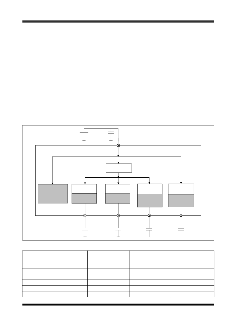
�2.1� Power� Supply� and� Ground� Block�
�Pins�
�To� provide� stable� sensitivity� and� linearity�
�characteristics� over� a� wide� supply� range,� the�
�MRF89XA� is� internally� voltage� regulated.� This� internal�
�regulated� power� supply� block� structure� is� illustrated� in�
�Figure� 2-2� .�
�The� power� supply� bypassing� is� essential� for� better�
�handling� of� signal� surges� and� noise� in� the� power� line.�
�To� ensure� correct� operation� of� the� regulator� circuit,� the�
�decoupling� capacitor� connection� (shown� in� Figure� 2-2� )�
�is� recommended.� These� decoupling� components� are�
�recommended� for� any� design.� The� power� supply� block�
�generates� four� regulated� supplies� for� the� analog,�
�digital,� VCO� and� the� PLL� blocks� to� reduce� the� voltages�
�for� their� specific� requirements.� However,� Power-on�
�Reset� (POR),� Configuration� registers� and� the� SPI� use�
�the� V� DD� supply� given� to� the� MRF89XA.�
�The� large� value� decoupling� capacitors� should� be�
�placed� at� the� PCB� power� input.� The� smaller� value�
�decoupling� capacitors� should� be� placed� at� every� power�
�point� of� the� device� and� at� bias� points� for� the� RF� port.�
�Poor� bypassing� can� lead� to� conducted� interference,�
�which� can� cause� noise� and� spurious� signals� to� couple�
�into� the� RF� sections,� thereby� significantly� reducing� the�
�performance.�
�It� is� recommended� that� the� V� DD� pin� have� two� bypass�
�capacitors� to� ensure� sufficient� bypass� and� decoupling.�
�However,� based� on� the� selected� carrier� frequency,� the�
�bypass� capacitor� values� vary.� The� trace� length� (V� DD� pin�
�to� bypass� capacitors)� should� be� made� as� short� as�
�possible.�
�FIGURE� 2-2:�
�POWER� SUPPLY� BLOCK� DIAGRAM�
�V� BAT�
�1� μF�
�Y5V�
�V� DD� –� Pin� 26�
�2.1� –� 3.6V�
�External� Supply�
�Internal� Regulator�
�1.4� V�
�V� INTS�
�Biasing:�
�-� SPI�
�-� Config.� Registers�
�-� POR�
�Analog� Regulator�
�1.0� V�
�Biasing� Analog�
�Blocks�
�AVRS�
�Pin� 27�
�1� μF�
�Y5V�
�Digital� Regulator�
�1.0� V�
�Biasing� Digital�
�Blocks�
�DVRS�
�Pin� 28�
�0.22� μF�
�X7R�
�VCO� Regulator�
�0.85� V�
�Biasing:�
�-� VCO� Circuit�
�-� Ext.� VCO� Tank�
�VCORS�
�Pin� 3�
�0.1� μF�
�X7R�
�PA� Regulator�
�1.80� V�
�Biasing:�
�-� PA� Driver�
�-� Ext.� PA� Choke�
�PARS�
�Pin� 29�
�0.047� μF�
�X7R�
�TABLE� 2-2:�
�POWER� SUPPLY� PIN� DETAILS�
�Blocks�
�POR,� SPI� and� Configuration� Registers�
�Regulated� Supply� (V� INTS� )�
�Analog�
�Digital�
�VCO�
�PA�
�Biasing� Through�
�V� DD�
�V� DD�
�V� INTS�
�V� INTS�
�V� INTS�
�V� DD�
�Associated� Pins�
�V� DD�
�V� DD�
�AVRS�
�DVRS�
�VCORS�
�PARS�
�Regulated� Voltage�
�(in� Volts)�
�2.1–3.6�
�1.4�
�1.0�
�1.0�
�0.85�
�1.8�
�DS70622C-page� 14�
�Preliminary�
�?� 2010–2011� Microchip� Technology� Inc.�
�相关PDF资料 |
PDF描述 |
|---|---|
| 241-5-12L | XFRMR PWR 115V 12.6VCT 1A LEADS |
| DPC-40-250 | XFRMR PWR 115/230V 40VCT 250MA |
| ST-5-56 | XFRMR PWR 115V 28V 440MA 12VA |
| 6221 | TIP STAIN-STEEL SHARP-PT .06"DMM |
| ST-5-48 | XFRMR PWR 115V 24V 500MA 12VA |
相关代理商/技术参数 |
参数描述 |
|---|---|
| MRF8HP21080HR3 | 功能描述:射频MOSFET电源晶体管 HV8 2.1GHZ 160W NI780H-4 RoHS:否 制造商:Freescale Semiconductor 配置:Single 晶体管极性: 频率:1800 MHz to 2000 MHz 增益:27 dB 输出功率:100 W 汲极/源极击穿电压: 漏极连续电流: 闸/源击穿电压: 最大工作温度: 封装 / 箱体:NI-780-4 封装:Tray |
| MRF8HP21080HR5 | 功能描述:射频MOSFET电源晶体管 HV8 2.1GHZ 160W NI780H-4 RoHS:否 制造商:Freescale Semiconductor 配置:Single 晶体管极性: 频率:1800 MHz to 2000 MHz 增益:27 dB 输出功率:100 W 汲极/源极击穿电压: 漏极连续电流: 闸/源击穿电压: 最大工作温度: 封装 / 箱体:NI-780-4 封装:Tray |
| MRF8HP21080HSR3 | 功能描述:射频MOSFET电源晶体管 HV8 2.1GHZ 160W NI780S-4 RoHS:否 制造商:Freescale Semiconductor 配置:Single 晶体管极性: 频率:1800 MHz to 2000 MHz 增益:27 dB 输出功率:100 W 汲极/源极击穿电压: 漏极连续电流: 闸/源击穿电压: 最大工作温度: 封装 / 箱体:NI-780-4 封装:Tray |
| MRF8HP21080HSR5 | 功能描述:射频MOSFET电源晶体管 HV8 2.1GHZ 160W NI780S-4 RoHS:否 制造商:Freescale Semiconductor 配置:Single 晶体管极性: 频率:1800 MHz to 2000 MHz 增益:27 dB 输出功率:100 W 汲极/源极击穿电压: 漏极连续电流: 闸/源击穿电压: 最大工作温度: 封装 / 箱体:NI-780-4 封装:Tray |
| MRF8HP21130HR3 | 功能描述:射频MOSFET电源晶体管 HV8 2.1GHZ 130W NI780-4 RoHS:否 制造商:Freescale Semiconductor 配置:Single 晶体管极性: 频率:1800 MHz to 2000 MHz 增益:27 dB 输出功率:100 W 汲极/源极击穿电压: 漏极连续电流: 闸/源击穿电压: 最大工作温度: 封装 / 箱体:NI-780-4 封装:Tray |
发布紧急采购,3分钟左右您将得到回复。