- 您现在的位置:买卖IC网 > PDF目录18765 > MRF89XAT-I/MQ (Microchip Technology)RF ISM BAND TXRX 32 QFN PDF资料下载
参数资料
| 型号: | MRF89XAT-I/MQ |
| 厂商: | Microchip Technology |
| 文件页数: | 15/140页 |
| 文件大小: | 0K |
| 描述: | RF ISM BAND TXRX 32 QFN |
| 标准包装: | 1 |
| 频率: | 863MHz ~ 870MHz,902MHz ~ 928MHz,950MHz ~ 960MHz |
| 数据传输率 - 最大: | 200kbps |
| 调制或协议: | FSK,OOK |
| 应用: | ISM |
| 功率 - 输出: | 12.5dBm |
| 灵敏度: | -113dBm |
| 电源电压: | 2.1 V ~ 3.6 V |
| 电流 - 接收: | 3mA |
| 电流 - 传输: | 25mA |
| 数据接口: | PCB,表面贴装 |
| 存储容量: | * |
| 天线连接器: | PCB,表面贴装 |
| 工作温度: | -40°C ~ 85°C |
| 封装/外壳: | 32-WFQFN 裸露焊盘 |
| 包装: | 标准包装 |
| 其它名称: | MRF89XAT-I/MQDKR |
第1页第2页第3页第4页第5页第6页第7页第8页第9页第10页第11页第12页第13页第14页当前第15页第16页第17页第18页第19页第20页第21页第22页第23页第24页第25页第26页第27页第28页第29页第30页第31页第32页第33页第34页第35页第36页第37页第38页第39页第40页第41页第42页第43页第44页第45页第46页第47页第48页第49页第50页第51页第52页第53页第54页第55页第56页第57页第58页第59页第60页第61页第62页第63页第64页第65页第66页第67页第68页第69页第70页第71页第72页第73页第74页第75页第76页第77页第78页第79页第80页第81页第82页第83页第84页第85页第86页第87页第88页第89页第90页第91页第92页第93页第94页第95页第96页第97页第98页第99页第100页第101页第102页第103页第104页第105页第106页第107页第108页第109页第110页第111页第112页第113页第114页第115页第116页第117页第118页第119页第120页第121页第122页第123页第124页第125页第126页第127页第128页第129页第130页第131页第132页第133页第134页第135页第136页第137页第138页第139页第140页
�� �
�
�MRF89XA�
�2.2� Reset� Pin�
�The� device� enters� the� Reset� mode� if� any� of� the�
�following� events� take� place:�
�The� PA� and� the� LNA� front-ends� in� the� MRF89XA,� which�
�share� the� same� Input/Output� pin,� are� internally�
�matched� to� approximately� 50� Ω� .�
�?� Power-on� Reset� (POR)�
�2.4�
�Filters� and� Amplifiers� Block�
�?� Manual� Reset�
�The� POR� happens� when� the� MRF89XA� is� switched� on�
�using� V� DD� .� The� POR� cycle� takes� at� least� 10� ms� to�
�execute� any� communication� operations� on� the� SPI� bus.�
�An� external� hardware� or� manual� Reset� of� the�
�MRF89XA� can� be� performed� by� asserting� the� TEST8�
�pin� (pin� 13)� to� high� for� 100� μs� and� then� releasing� the�
�pin.� After� releasing� the� pin,� it� takes� more� than� 5� ms� for�
�the� transceiver� to� be� ready� for� any� operations.� The� pin�
�is� driven� with� an� open-drain� output,� therefore,� is� pulled�
�high� while� the� device� is� in� POR.� The� device� will� not�
�accept� commands� during� the� Reset� period.� For� more�
�information,� refer� to� Section� 3.1.2,� Manual� Reset� .�
�2.4.1� INTERPOLATION� FILTER�
�After� digital-to-analog� conversion� during� transmission,�
�both� I� and� Q� signals� are� smoothed� by� interpolation�
�filters.� These� low-pass� filters� the� digitally� generated�
�signal,� and� prevents� the� alias� signals� from� entering� the�
�modulators.�
�2.4.2� POWER� AMPLIFIER�
�The� Power� Amplifier� (PA)� integrated� in� the� MRF89XA�
�operates� under� a� regulated� voltage� supply� of� 1.8V.� The�
�external� RF� choke� inductor� is� biased� by� an� internal�
�regulator� output� made� available� on� the� PARS� pin� (pin�
�29).� Therefore,� the� PA� output� power� is� consistent� over�
�2.3�
�RFIO� Pin�
�the� power� supply� range.� This� is� important� for�
�applications� which� allows� both� predictable� RF�
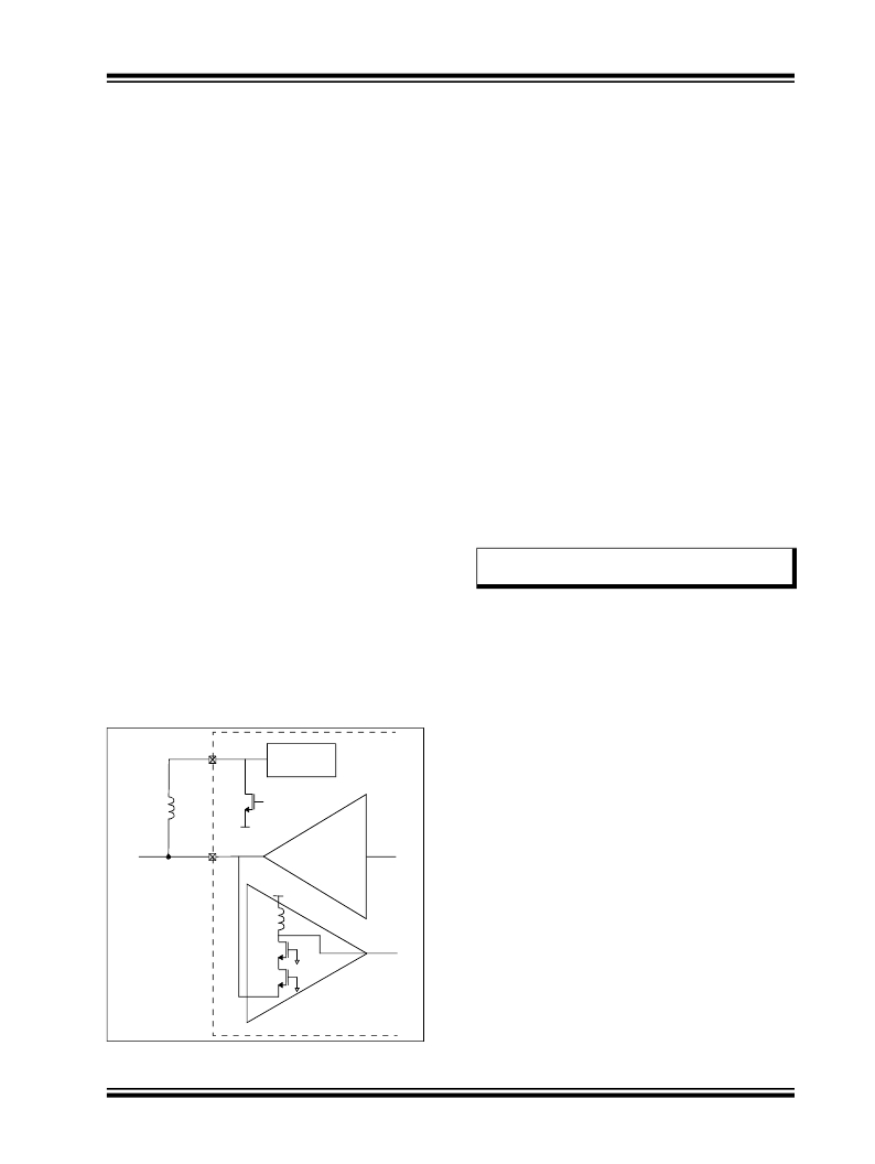
�The� receiver� and� the� transmitter� share� the� same� RFIO�
�pin� (pin� 31).� Figure� 2-3� illustrates� the� configuration� of�
�the� common� RF� front-end.�
�?� In� Transmit� mode,� the� PA� and� the� PA� regulator�
�are� ON� with� voltage� on� the� PARS� pin� (pin� 29)�
�performance� and� battery� life.�
�An� open� collector� output� requires� biasing� using� an�
�inductor� as� an� RF� choke.� For� the� recommended� PA�
�bias� and� matching� circuit� details� see� Section� 4.4.2,�
�Suggested� PA� Biasing� And� Matching� .�
�equal� to� the� nominal� voltage� of� the� regulator�
�(about� 1.8V).� The� external� RF� choke� inductance�
�is� used� to� bias� the� PA.�
�Note:�
�Image� rejection� is� achieved� using� a� SAW�
�filter� on� the� RF� input.�
�?� In� Receive� mode,� the� PA� and� PA� regulator� are�
�OFF� and� PARS� is� tied� to� ground.� The� external� RF�
�choke� inductor� is� used� for� biasing� and� matching�
�the� LNA� (this� is� basically� implemented� as� a� com-�
�mon� gate� amplifier).�
�The� matching� of� the� SAW� filter� depends� on� the� SAW�
�filter� selected.� Many� modern� SAW� filters� have� 50� Ω�
�input� and� output,� which� simplifies� matching� for� the�
�MRF89XA.� This� is� demonstrated� in� the� application�
�circuit.� If� the� choice� of� SAW� filter� is� different� than� 50� Ω� ,�
�the� required� impedance� match� on� the� input� and� output�
�FIGURE� 2-3:�
�COMMON� RF� INPUT� AND�
�of� the� SAW� filter� will� be� needed.�
�OUTPUT� PIN� DIAGRAM�
�2.4.3�
�LOW� NOISE� AMPLIFIER�
�(WITH�
�PARS�
�PA� Regulator�
�(1.8V)�
�RX� ON�
�FIRST� MIXER)�
�In� Receive� mode,� the� RFIO� pin� (pin� 31)� is� connected� to�
�a� fixed� gain,� common-gate,� Low� Noise� Amplifier� (LNA).�
�The� performance� of� this� amplifier� is� such� that� the� Noise�
�Figure� (NF)� of� the� receiver� is� estimated� to� be�
�approximately� 7� dB.�
�To�
�Antenna�
�RFIO�
�PA�
�The� LNA� has� approximately� 50� Ω� impedance,� which�
�functions� well� with� the� proposed� antenna� (PCB/�
�Monopole)� during� signal� transmission.� The� LNA� is� fol-�
�lowed� by� an� internal� RF� band-pass� filter.�
�LNA�
�?� 2010–2011� Microchip� Technology� Inc.�
�Preliminary�
�DS70622C-page� 15�
�相关PDF资料 |
PDF描述 |
|---|---|
| 241-5-12L | XFRMR PWR 115V 12.6VCT 1A LEADS |
| DPC-40-250 | XFRMR PWR 115/230V 40VCT 250MA |
| ST-5-56 | XFRMR PWR 115V 28V 440MA 12VA |
| 6221 | TIP STAIN-STEEL SHARP-PT .06"DMM |
| ST-5-48 | XFRMR PWR 115V 24V 500MA 12VA |
相关代理商/技术参数 |
参数描述 |
|---|---|
| MRF8HP21080HR3 | 功能描述:射频MOSFET电源晶体管 HV8 2.1GHZ 160W NI780H-4 RoHS:否 制造商:Freescale Semiconductor 配置:Single 晶体管极性: 频率:1800 MHz to 2000 MHz 增益:27 dB 输出功率:100 W 汲极/源极击穿电压: 漏极连续电流: 闸/源击穿电压: 最大工作温度: 封装 / 箱体:NI-780-4 封装:Tray |
| MRF8HP21080HR5 | 功能描述:射频MOSFET电源晶体管 HV8 2.1GHZ 160W NI780H-4 RoHS:否 制造商:Freescale Semiconductor 配置:Single 晶体管极性: 频率:1800 MHz to 2000 MHz 增益:27 dB 输出功率:100 W 汲极/源极击穿电压: 漏极连续电流: 闸/源击穿电压: 最大工作温度: 封装 / 箱体:NI-780-4 封装:Tray |
| MRF8HP21080HSR3 | 功能描述:射频MOSFET电源晶体管 HV8 2.1GHZ 160W NI780S-4 RoHS:否 制造商:Freescale Semiconductor 配置:Single 晶体管极性: 频率:1800 MHz to 2000 MHz 增益:27 dB 输出功率:100 W 汲极/源极击穿电压: 漏极连续电流: 闸/源击穿电压: 最大工作温度: 封装 / 箱体:NI-780-4 封装:Tray |
| MRF8HP21080HSR5 | 功能描述:射频MOSFET电源晶体管 HV8 2.1GHZ 160W NI780S-4 RoHS:否 制造商:Freescale Semiconductor 配置:Single 晶体管极性: 频率:1800 MHz to 2000 MHz 增益:27 dB 输出功率:100 W 汲极/源极击穿电压: 漏极连续电流: 闸/源击穿电压: 最大工作温度: 封装 / 箱体:NI-780-4 封装:Tray |
| MRF8HP21130HR3 | 功能描述:射频MOSFET电源晶体管 HV8 2.1GHZ 130W NI780-4 RoHS:否 制造商:Freescale Semiconductor 配置:Single 晶体管极性: 频率:1800 MHz to 2000 MHz 增益:27 dB 输出功率:100 W 汲极/源极击穿电压: 漏极连续电流: 闸/源击穿电压: 最大工作温度: 封装 / 箱体:NI-780-4 封装:Tray |
发布紧急采购,3分钟左右您将得到回复。