- 您现在的位置:买卖IC网 > PDF目录18765 > MRF89XAT-I/MQ (Microchip Technology)RF ISM BAND TXRX 32 QFN PDF资料下载
参数资料
| 型号: | MRF89XAT-I/MQ |
| 厂商: | Microchip Technology |
| 文件页数: | 20/140页 |
| 文件大小: | 0K |
| 描述: | RF ISM BAND TXRX 32 QFN |
| 标准包装: | 1 |
| 频率: | 863MHz ~ 870MHz,902MHz ~ 928MHz,950MHz ~ 960MHz |
| 数据传输率 - 最大: | 200kbps |
| 调制或协议: | FSK,OOK |
| 应用: | ISM |
| 功率 - 输出: | 12.5dBm |
| 灵敏度: | -113dBm |
| 电源电压: | 2.1 V ~ 3.6 V |
| 电流 - 接收: | 3mA |
| 电流 - 传输: | 25mA |
| 数据接口: | PCB,表面贴装 |
| 存储容量: | * |
| 天线连接器: | PCB,表面贴装 |
| 工作温度: | -40°C ~ 85°C |
| 封装/外壳: | 32-WFQFN 裸露焊盘 |
| 包装: | 标准包装 |
| 其它名称: | MRF89XAT-I/MQDKR |
第1页第2页第3页第4页第5页第6页第7页第8页第9页第10页第11页第12页第13页第14页第15页第16页第17页第18页第19页当前第20页第21页第22页第23页第24页第25页第26页第27页第28页第29页第30页第31页第32页第33页第34页第35页第36页第37页第38页第39页第40页第41页第42页第43页第44页第45页第46页第47页第48页第49页第50页第51页第52页第53页第54页第55页第56页第57页第58页第59页第60页第61页第62页第63页第64页第65页第66页第67页第68页第69页第70页第71页第72页第73页第74页第75页第76页第77页第78页第79页第80页第81页第82页第83页第84页第85页第86页第87页第88页第89页第90页第91页第92页第93页第94页第95页第96页第97页第98页第99页第100页第101页第102页第103页第104页第105页第106页第107页第108页第109页第110页第111页第112页第113页第114页第115页第116页第117页第118页第119页第120页第121页第122页第123页第124页第125页第126页第127页第128页第129页第130页第131页第132页第133页第134页第135页第136页第137页第138页第139页第140页
�� �
�
�MRF89XA�
�2.9.1�
�TRANSMITTER� ARCHITECTURE�
�In� OOK� mode,� the� phase� difference� between� the� I� and�
�Figure� 2-6� illustrates� the� transmitter� architecture� block�
�diagram.� The� baseband� I� and� Q� signals� are� digitally�
�generated� by� a� DDS� whose� Digital-to-Analog�
�Converters� (DAC)� followed� by� two� anti-aliasing� low-�
�pass� filters� transform� the� digital� signal� into� analog� in-�
�phase� (I)� and� quadrature� (Q)� components� whose�
�frequency� is� the� selected� frequency� deviation,� is� set�
�using� the� FDVAL<7:0>� bits� from� FDEVREG<7:0>.�
�In� FSK� mode,� the� relative� phase� of� I� and� Q� is� switched�
�by� the� input� data� between� -90°� and� +90°� with� continu-�
�ous� phase.� The� modulation� is� therefore� performed� at�
�this� initial� stage,� because� the� information� contained� in�
�the� phase� difference� will� be� converted� into� a� frequency�
�shift� when� the� I� and� Q� signals� are� up-converted� in� the�
�first� mixer� stage.� This� first� up-conversion� stage� is� dupli-�
�cated� to� enhance� image� rejection.� The� FSK� convention�
�is� such� that:�
�DATA� =� 1� →� f� rf� +� f� dev�
�DATA� =� 0� →� f� rf� –� f� dev�
�Q� channels� is� kept� constant� (independent� of� the�
�transmitted� data).� Thus,� the� first� stage� of� up-conversion�
�creates� a� fixed� frequency� signal� at� the� low� IF� =� f� dev� (this�
�explains� why� the� transmitted� OOK� spectrum� is� offset� by�
�f� dev� ).� OOK� Modulation� is� accomplished� by� switching� the�
�PA� and� PA� regulator� stages� ON� and� OFF.� By�
�convention:�
�DATA� =� 1� →� PAon�
�DATA� =� 0� →� PAoff�
�After� the� interpolation� filters,� a� set� of� four� mixers�
�combines� the� I� and� Q� signals� and� converts� them� into� a�
�pair� of� complex� signals� at� the� second� intermediate�
�frequency,� equal� to� one-eighth� of� the� LO� frequency,� or�
�one-ninth� of� the� RF� frequency.� These� two� new� I� and� Q�
�signals� are� then� combined� and� up-converted� to� the�
�final� RF� frequency� by� two� quadrature� mixers� fed� by� the�
�LO� signal.� The� signal� is� pre-amplified,� and� then� the�
�transmitter� output� is� driven� by� a� final� power� amplifier�
�stage.� The� I� and� Q� signal� details� are� illustrated� in�
�Figure� 2-7� .�
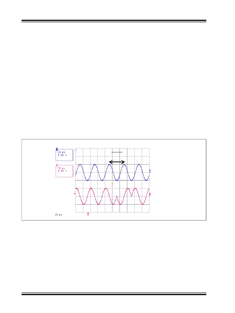
�FIGURE� 2-7:�
�I(t),� Q(t)� Signals� Overview�
�1�
�Fdev�
�I(t)�
�Q(t)�
�DS70622C-page� 20�
�Preliminary�
�?� 2010–2011� Microchip� Technology� Inc.�
�相关PDF资料 |
PDF描述 |
|---|---|
| 241-5-12L | XFRMR PWR 115V 12.6VCT 1A LEADS |
| DPC-40-250 | XFRMR PWR 115/230V 40VCT 250MA |
| ST-5-56 | XFRMR PWR 115V 28V 440MA 12VA |
| 6221 | TIP STAIN-STEEL SHARP-PT .06"DMM |
| ST-5-48 | XFRMR PWR 115V 24V 500MA 12VA |
相关代理商/技术参数 |
参数描述 |
|---|---|
| MRF8HP21080HR3 | 功能描述:射频MOSFET电源晶体管 HV8 2.1GHZ 160W NI780H-4 RoHS:否 制造商:Freescale Semiconductor 配置:Single 晶体管极性: 频率:1800 MHz to 2000 MHz 增益:27 dB 输出功率:100 W 汲极/源极击穿电压: 漏极连续电流: 闸/源击穿电压: 最大工作温度: 封装 / 箱体:NI-780-4 封装:Tray |
| MRF8HP21080HR5 | 功能描述:射频MOSFET电源晶体管 HV8 2.1GHZ 160W NI780H-4 RoHS:否 制造商:Freescale Semiconductor 配置:Single 晶体管极性: 频率:1800 MHz to 2000 MHz 增益:27 dB 输出功率:100 W 汲极/源极击穿电压: 漏极连续电流: 闸/源击穿电压: 最大工作温度: 封装 / 箱体:NI-780-4 封装:Tray |
| MRF8HP21080HSR3 | 功能描述:射频MOSFET电源晶体管 HV8 2.1GHZ 160W NI780S-4 RoHS:否 制造商:Freescale Semiconductor 配置:Single 晶体管极性: 频率:1800 MHz to 2000 MHz 增益:27 dB 输出功率:100 W 汲极/源极击穿电压: 漏极连续电流: 闸/源击穿电压: 最大工作温度: 封装 / 箱体:NI-780-4 封装:Tray |
| MRF8HP21080HSR5 | 功能描述:射频MOSFET电源晶体管 HV8 2.1GHZ 160W NI780S-4 RoHS:否 制造商:Freescale Semiconductor 配置:Single 晶体管极性: 频率:1800 MHz to 2000 MHz 增益:27 dB 输出功率:100 W 汲极/源极击穿电压: 漏极连续电流: 闸/源击穿电压: 最大工作温度: 封装 / 箱体:NI-780-4 封装:Tray |
| MRF8HP21130HR3 | 功能描述:射频MOSFET电源晶体管 HV8 2.1GHZ 130W NI780-4 RoHS:否 制造商:Freescale Semiconductor 配置:Single 晶体管极性: 频率:1800 MHz to 2000 MHz 增益:27 dB 输出功率:100 W 汲极/源极击穿电压: 漏极连续电流: 闸/源击穿电压: 最大工作温度: 封装 / 箱体:NI-780-4 封装:Tray |
发布紧急采购,3分钟左右您将得到回复。