- 您现在的位置:买卖IC网 > PDF目录229297 > MT46V32M8BG-6AT:G 32M X 8 DDR DRAM, 0.7 ns, PBGA60 PDF资料下载
参数资料
| 型号: | MT46V32M8BG-6AT:G |
| 元件分类: | DRAM |
| 英文描述: | 32M X 8 DDR DRAM, 0.7 ns, PBGA60 |
| 封装: | (8 X 14) MM, LEAD FREE,PLASTIC, FBGA-60 |
| 文件页数: | 11/93页 |
| 文件大小: | 3632K |
第1页第2页第3页第4页第5页第6页第7页第8页第9页第10页当前第11页第12页第13页第14页第15页第16页第17页第18页第19页第20页第21页第22页第23页第24页第25页第26页第27页第28页第29页第30页第31页第32页第33页第34页第35页第36页第37页第38页第39页第40页第41页第42页第43页第44页第45页第46页第47页第48页第49页第50页第51页第52页第53页第54页第55页第56页第57页第58页第59页第60页第61页第62页第63页第64页第65页第66页第67页第68页第69页第70页第71页第72页第73页第74页第75页第76页第77页第78页第79页第80页第81页第82页第83页第84页第85页第86页第87页第88页第89页第90页第91页第92页第93页
PDF: 09005aef80768abb/Source: 09005aef82a95a3a
Micron Technology, Inc., reserves the right to change products or specifications without notice.
256Mb_DDR_x4x8x16_D2.fm - 256Mb DDR: Rev. O, Core DDR: Rev. B 1/09 EN
19
2003 Micron Technology, Inc. All rights reserved.
256Mb: x4, x8, x16 DDR SDRAM
Electrical Specifications – IDD
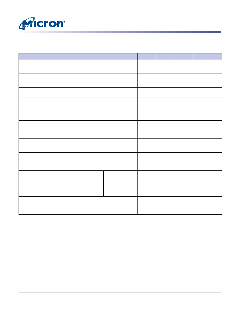
Table 8:
IDD Specifications and Conditions (x4, x8, x16: -5B, -6, -6T) - Die Revision K Only
VDDQ = +2.6V ±0.1V, VDD = +2.6V ±0.1V (-5B); VDDQ = +2.5V ±0.2V, VDD = +2.5V ±0.2V (-6, -6T);
0°C
≤ T
Parameter/Condition
Symbol
-5B
-6/6T
Units
Notes
Operating one-bank precharge current: tRC = tRC (MIN);
tCK = tCK (MIN); DQ, DM, and DQS inputs changing once per clock
cycle; Address and control inputs changing once every two clock cycles
IDD0
100
90
mA
Operating one-bank active-read-precharge current: Burst = 4;
tRC = tRC (MIN); tCK = tCK (MIN); IOUT = 0mA; Address and control
inputs changing once per clock cycle
IDD1
120
115
mA
Precharge power-down standby current: All banks idle; Power-
down mode; tCK = tCK (MIN); CKE = LOW
IDD2P
4
mA
Idle standby current: CS# = HIGH; All banks are idle; tCK = tCK (MIN);
CKE = HIGH; Address and other control inputs changing once per clock
cycle; VIN =VREF for DQ, DQS, and DM
IDD2F
50
mA
Active power-down standby current: One bank active; Power-
down mode; tCK = tCK (MIN); CKE = LOW
IDD3P
35
30
mA
Active standby current: CS# = HIGH; CKE = HIGH; One bank active;
tRC = tRAS (MAX); tCK = tCK (MIN); DQ, DM, and DQS inputs changing
twice per clock cycle; Address and other control inputs changing once
per clock cycle
IDD3N
60
55
mA
Operating burst read current: Burst = 2; Continuous burst reads;
One bank active; Address and control inputs changing once per clock
cycle; tCK = tCK (MIN);
IOUT =0mA
IDD4R
180
160
mA
Operating burst write current: Burst = 2; Continuous burst writes;
One bank active; Address and control inputs changing once per clock
cycle; tCK = tCK (MIN); DQ, DM, and DQS inputs changing twice per
clock cycle
IDD4W
180
160
mA
Auto refresh burst current:
tREFC = tRFC (MIN)
IDD5
160
mA
tREFC = 7.8s
IDD5A
6
mA
tREFC = 1.95s (AT)
IDD5A
9
mA
Self refresh current: CKE
≤ 0.2V
Standard
IDD64
4
mA
Low power (L)
IDD6A
2
mA
Operating bank interleave read current: Four-bank interleaving
READs (burst = 4) with auto precharge; tRC = minimum tRC allowed;
tCK = tCK (MIN); Address and control inputs change only during
ACTIVE, READ, or WRITE commands
IDD7
290
270
mA
相关PDF资料 |
PDF描述 |
|---|---|
| M29F800FB55N3E2 | 512K X 16 FLASH 5V PROM, 55 ns, PDSO48 |
| MC12L1NZGF | ROTARY SWITCH-12POSITIONS, SP12T, LATCHED, 0.25A, 28VDC, PANEL MOUNT-THREADED |
| MD00S1NCQF | ROTARY SWITCH-6POSITIONS, DP6T, LATCHED, 0.25A, 28VDC, THROUGH HOLE-STRAIGHT |
| MD06L1NZGD | ROTARY SWITCH-6POSITIONS, DP6T, LATCHED, 0.25A, 28VDC, PANEL MOUNT-THREADED |
| MD06L2NCQD | ROTARY SWITCH-6POSITIONS, DP6T, LATCHED, 0.25A, 28VDC, THROUGH HOLE-STRAIGHT |
相关代理商/技术参数 |
参数描述 |
|---|
发布紧急采购,3分钟左右您将得到回复。