- 您现在的位置:买卖IC网 > PDF目录299581 > ORLI10G1BM680-DB (LATTICE SEMICONDUCTOR CORP) FPGA, 1296 CLBS, 333000 GATES, PBGA680 PDF资料下载
参数资料
| 型号: | ORLI10G1BM680-DB |
| 厂商: | LATTICE SEMICONDUCTOR CORP |
| 元件分类: | FPGA |
| 英文描述: | FPGA, 1296 CLBS, 333000 GATES, PBGA680 |
| 封装: | PLASTIC, FBGA-680 |
| 文件页数: | 22/78页 |
| 文件大小: | 1689K |
| 代理商: | ORLI10G1BM680-DB |
第1页第2页第3页第4页第5页第6页第7页第8页第9页第10页第11页第12页第13页第14页第15页第16页第17页第18页第19页第20页第21页当前第22页第23页第24页第25页第26页第27页第28页第29页第30页第31页第32页第33页第34页第35页第36页第37页第38页第39页第40页第41页第42页第43页第44页第45页第46页第47页第48页第49页第50页第51页第52页第53页第54页第55页第56页第57页第58页第59页第60页第61页第62页第63页第64页第65页第66页第67页第68页第69页第70页第71页第72页第73页第74页第75页第76页第77页第78页
Lattice Semiconductor
ORCA ORLI10G Data Sheet
29
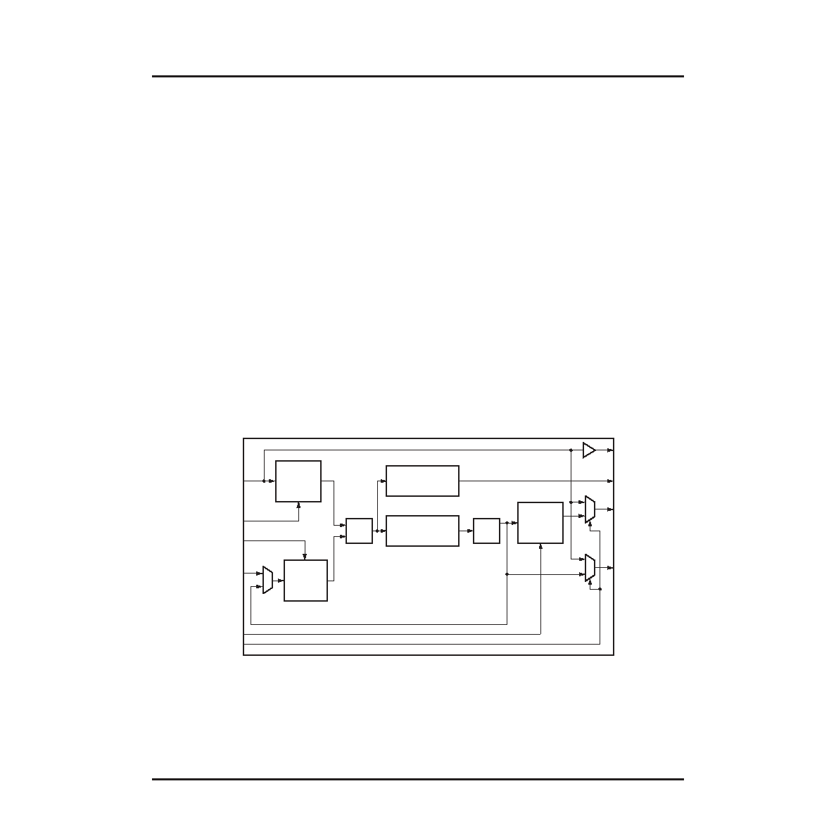
ORLI10G Embedded PLLs
The ORLI10G embedded (transmit and receive) PLLs are based on the 4E series FPGA High-Speed Programma-
ble PLL (HPPLL). The 4E PLL consists of a Phase/Frequency Detector (PFD), a charge pump/lter, a multitap Volt-
age Controlled Oscillator (VCO), a duty cycle synthesis circuitry, a power regulator, two programmable dividers,
phase shift selector multiplexers, a lock signal generator, and a current DAC. A block diagram of the programmable
PLL is shown in Figure 16. The receive path RX1_PLL and transmit path TX1_PLL, which can be programmed to
create a N/M frequency clock, are based on this design.
The receive path RX2_PLL and transmit path TX2_PLL create a X1 clock. This is essentially the same PLL without
the M and N divider.
The RCKI input to the PLLs comes from an input clock to the ORLI10G that has been divided in frequency by either
4 or 8 (programmable). As shown in Figure 4, RX1_PLL and RX2_PLL are driven by the divided version of
RX_CLK_IN0. As shown in Figure 5, TX1_PLL and TX2_PLL are driven by the divided versions of TX_CLK_IN. It
should be noted that the speed of the ORLI10G line interface is therefore either 4x or 8x the operating speed of the
embedded PLLs.
The clock feedback loops for the RX2_PLL and TX2_PLL should be routed from the clock network in the FPGA
core to compensate for the routing delays to the FPGA logic interface. The source to the TX2_FBCKI or
RX2_FBCKI inputs must come from an FPGA clock network driven by the VCO output (otherwise, any phase shift-
ing on VCOP is removed by the feedback loops). In this way, the clock skew at the embedded core/FPGA logic
boundary is zero for the receive and transmit PLLs.
All PLLs include a phase shift selector which allows phase shift adjustments of each clock in increments of 1/8 the
period of the clock. This phase shifted output is available on the VCOP output of the PLL. All functions of the
embedded core PLLs are user controlled through a GUI provided with the ORLI10G design kit software.
Figure 16. ORLI10G Programmable PLL Block Diagram
RCKI
M<5:0>
N<5:0>
SEL<2:0>
BYPASS
M
DIVIDER
N
DIVIDER
PFD
LOCK
GENERATOR
CHARGE PUMP
AND FILTER
VCO
PHASE
SELECT
RCKO
LOCK
VCOP
VCO
TX2_FBCKI
RX2_FBCKI
相关PDF资料 |
PDF描述 |
|---|---|
| ORLI10G2BM680-DB | FPGA, 1296 CLBS, 333000 GATES, PBGA680 |
| ORLI10G3BM680-DB | FPGA, 1296 CLBS, 333000 GATES, PBGA680 |
| ORT82G5-1BM680 | FPGA, 1296 CLBS, 380000 GATES, PBGA680 |
| ORT82G5-2BM680 | FPGA, 1296 CLBS, 380000 GATES, PBGA680 |
| ORT82G5-3BM680 | FPGA, 1296 CLBS, 380000 GATES, PBGA680 |
相关代理商/技术参数 |
参数描述 |
|---|---|
| ORLI10G-1BM680I | 功能描述:FPGA - 现场可编程门阵列 10368 LUT 316 I/O RoHS:否 制造商:Altera Corporation 系列:Cyclone V E 栅极数量: 逻辑块数量:943 内嵌式块RAM - EBR:1956 kbit 输入/输出端数量:128 最大工作频率:800 MHz 工作电源电压:1.1 V 最大工作温度:+ 70 C 安装风格:SMD/SMT 封装 / 箱体:FBGA-256 |
| ORLI10G-1BMN680C | 功能描述:FPGA - 现场可编程门阵列 10368 LUT 316 I/O RoHS:否 制造商:Altera Corporation 系列:Cyclone V E 栅极数量: 逻辑块数量:943 内嵌式块RAM - EBR:1956 kbit 输入/输出端数量:128 最大工作频率:800 MHz 工作电源电压:1.1 V 最大工作温度:+ 70 C 安装风格:SMD/SMT 封装 / 箱体:FBGA-256 |
| ORLI10G-1BMN680I | 功能描述:FPGA - 现场可编程门阵列 10368 LUT 316 I/O RoHS:否 制造商:Altera Corporation 系列:Cyclone V E 栅极数量: 逻辑块数量:943 内嵌式块RAM - EBR:1956 kbit 输入/输出端数量:128 最大工作频率:800 MHz 工作电源电压:1.1 V 最大工作温度:+ 70 C 安装风格:SMD/SMT 封装 / 箱体:FBGA-256 |
| ORLI10G-2BM680C | 功能描述:FPGA - 现场可编程门阵列 10368 LUT 316 I/O RoHS:否 制造商:Altera Corporation 系列:Cyclone V E 栅极数量: 逻辑块数量:943 内嵌式块RAM - EBR:1956 kbit 输入/输出端数量:128 最大工作频率:800 MHz 工作电源电压:1.1 V 最大工作温度:+ 70 C 安装风格:SMD/SMT 封装 / 箱体:FBGA-256 |
| ORLI10G-2BM680I | 功能描述:FPGA - 现场可编程门阵列 10368 LUT 316 I/O RoHS:否 制造商:Altera Corporation 系列:Cyclone V E 栅极数量: 逻辑块数量:943 内嵌式块RAM - EBR:1956 kbit 输入/输出端数量:128 最大工作频率:800 MHz 工作电源电压:1.1 V 最大工作温度:+ 70 C 安装风格:SMD/SMT 封装 / 箱体:FBGA-256 |
发布紧急采购,3分钟左右您将得到回复。