- 您现在的位置:买卖IC网 > PDF目录299581 > ORLI10G1BM680-DB (LATTICE SEMICONDUCTOR CORP) FPGA, 1296 CLBS, 333000 GATES, PBGA680 PDF资料下载
参数资料
| 型号: | ORLI10G1BM680-DB |
| 厂商: | LATTICE SEMICONDUCTOR CORP |
| 元件分类: | FPGA |
| 英文描述: | FPGA, 1296 CLBS, 333000 GATES, PBGA680 |
| 封装: | PLASTIC, FBGA-680 |
| 文件页数: | 8/78页 |
| 文件大小: | 1689K |
| 代理商: | ORLI10G1BM680-DB |
第1页第2页第3页第4页第5页第6页第7页当前第8页第9页第10页第11页第12页第13页第14页第15页第16页第17页第18页第19页第20页第21页第22页第23页第24页第25页第26页第27页第28页第29页第30页第31页第32页第33页第34页第35页第36页第37页第38页第39页第40页第41页第42页第43页第44页第45页第46页第47页第48页第49页第50页第51页第52页第53页第54页第55页第56页第57页第58页第59页第60页第61页第62页第63页第64页第65页第66页第67页第68页第69页第70页第71页第72页第73页第74页第75页第76页第77页第78页
Lattice Semiconductor
ORCA ORLI10G Data Sheet
16
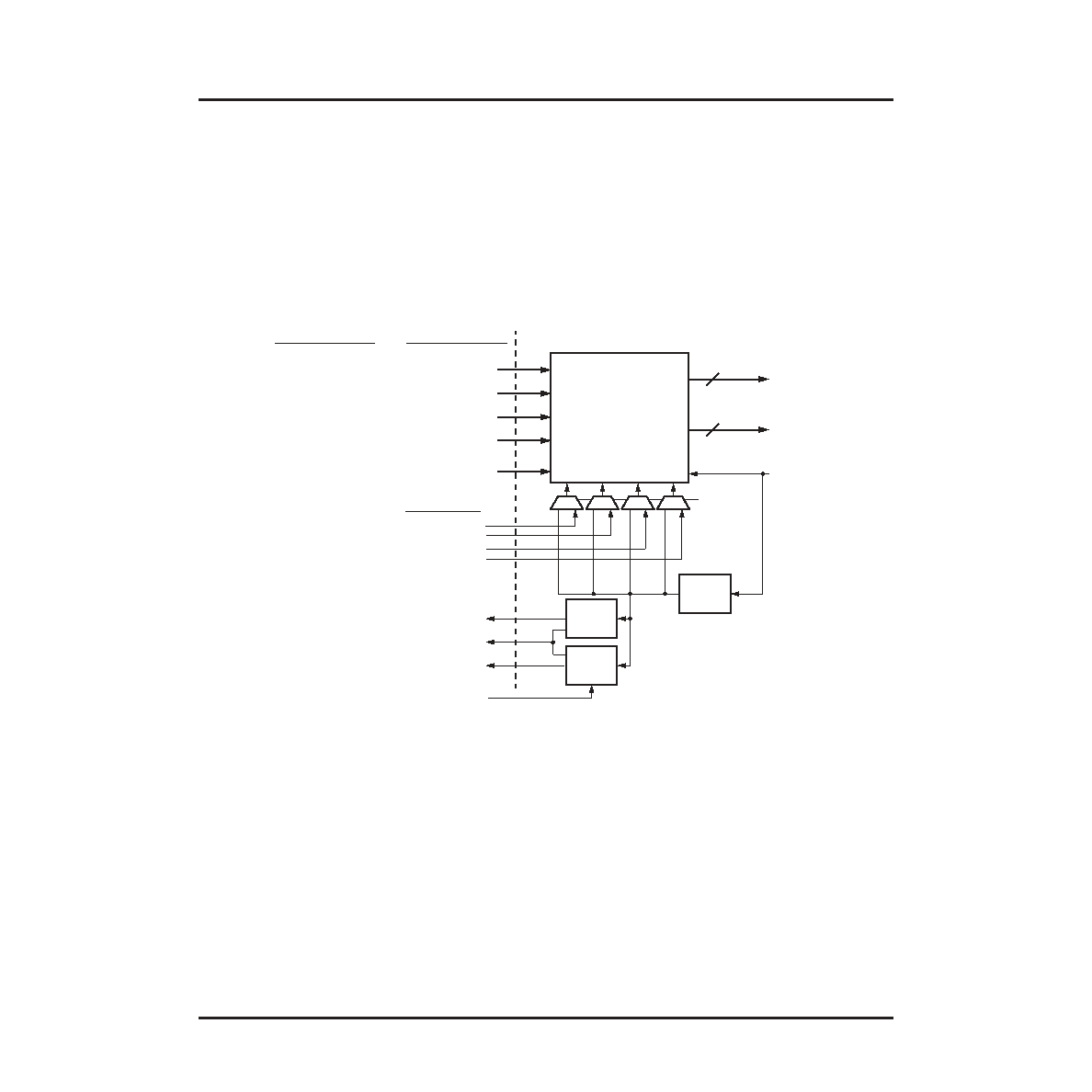
The transmit line interface on the ORLI10G can connect to devices that are compliant to either the XSBI standard
or the SFI-4 standard. The major difference for these standards is that for XSBI, the least signicant bit [0] is trans-
ferred rst after serialization by the external MUX device, whereas SFI-4 transmits the most signicant bit rst. In
some cases, bits [15:0] on the ORLI10G should connect to bits [0:15] on the device to which the ORLI10G device
interfaces. An example of this is the PCS IP core in the ORLI10G when the ORLI10G is connected to an XSBI ver-
sion 2.1 device.
It should be noted that IEEE 802.3ae version 3.1 to D3.4 (version D3.4 is the latest draft version of this specica-
tion as of the writing of this data sheet) swaps XSBI so that the most signicant bit is transferred rst, thus requiring
that bits [0:15] on the ORLI10G be connected directly to bits [0:15] on the XSBI device.
Figure 5. ORLI10G Embedded Core Transmit Path Diagram
Note: TX_ENB8_IN[3:0] and TX_CLK8_IN[3:0] are generally not used. See text for explanation.
128 TO 16 MUX
OR
64 TO 16 MUX
DATA
TX_DAT_OUT
16
CLOCK
TX_CLK8_OUT
4
TRANSMIT REFERENCE
CLOCK
FPGA LOGIC
DIVIDE BY 8 MODE
TX_DAT_IN[127:96]
TX_DAT_IN[95:64]
TX_DAT_IN[63:32]
TX_DAT_IN[31:0]
OR
TX_ENB8_IN[3:0]
DIVIDE BY 4 MODE
TX_DAT_IN[111:96]
TX_DAT_IN[79:64]
TX_DAT_IN[47:32]
TX_DAT_IN[15:0]
INTCLK
TX_CLK8_IN[0]
TX_CLK8_IN[1]
TX_CLK8_IN[2]
TX_CLK8_IN[3]
DIV BY 8
OR
DIV BY 4
TX_CLK_IN
ORLI10G CORE
TX1_PLL
(M/N)
TX2_PLL
(X1)
TX1_VCOP (X M/N CLOCK)
TX_LOCK
TX2_VCOP (X 1 CLOCK)
TX_ENB8_IN[3:0]
TX1_VCO
TX2_VCO
BOTH MODES
TX2_FBCKI
EXTCLK
相关PDF资料 |
PDF描述 |
|---|---|
| ORLI10G2BM680-DB | FPGA, 1296 CLBS, 333000 GATES, PBGA680 |
| ORLI10G3BM680-DB | FPGA, 1296 CLBS, 333000 GATES, PBGA680 |
| ORT82G5-1BM680 | FPGA, 1296 CLBS, 380000 GATES, PBGA680 |
| ORT82G5-2BM680 | FPGA, 1296 CLBS, 380000 GATES, PBGA680 |
| ORT82G5-3BM680 | FPGA, 1296 CLBS, 380000 GATES, PBGA680 |
相关代理商/技术参数 |
参数描述 |
|---|---|
| ORLI10G-1BM680I | 功能描述:FPGA - 现场可编程门阵列 10368 LUT 316 I/O RoHS:否 制造商:Altera Corporation 系列:Cyclone V E 栅极数量: 逻辑块数量:943 内嵌式块RAM - EBR:1956 kbit 输入/输出端数量:128 最大工作频率:800 MHz 工作电源电压:1.1 V 最大工作温度:+ 70 C 安装风格:SMD/SMT 封装 / 箱体:FBGA-256 |
| ORLI10G-1BMN680C | 功能描述:FPGA - 现场可编程门阵列 10368 LUT 316 I/O RoHS:否 制造商:Altera Corporation 系列:Cyclone V E 栅极数量: 逻辑块数量:943 内嵌式块RAM - EBR:1956 kbit 输入/输出端数量:128 最大工作频率:800 MHz 工作电源电压:1.1 V 最大工作温度:+ 70 C 安装风格:SMD/SMT 封装 / 箱体:FBGA-256 |
| ORLI10G-1BMN680I | 功能描述:FPGA - 现场可编程门阵列 10368 LUT 316 I/O RoHS:否 制造商:Altera Corporation 系列:Cyclone V E 栅极数量: 逻辑块数量:943 内嵌式块RAM - EBR:1956 kbit 输入/输出端数量:128 最大工作频率:800 MHz 工作电源电压:1.1 V 最大工作温度:+ 70 C 安装风格:SMD/SMT 封装 / 箱体:FBGA-256 |
| ORLI10G-2BM680C | 功能描述:FPGA - 现场可编程门阵列 10368 LUT 316 I/O RoHS:否 制造商:Altera Corporation 系列:Cyclone V E 栅极数量: 逻辑块数量:943 内嵌式块RAM - EBR:1956 kbit 输入/输出端数量:128 最大工作频率:800 MHz 工作电源电压:1.1 V 最大工作温度:+ 70 C 安装风格:SMD/SMT 封装 / 箱体:FBGA-256 |
| ORLI10G-2BM680I | 功能描述:FPGA - 现场可编程门阵列 10368 LUT 316 I/O RoHS:否 制造商:Altera Corporation 系列:Cyclone V E 栅极数量: 逻辑块数量:943 内嵌式块RAM - EBR:1956 kbit 输入/输出端数量:128 最大工作频率:800 MHz 工作电源电压:1.1 V 最大工作温度:+ 70 C 安装风格:SMD/SMT 封装 / 箱体:FBGA-256 |
发布紧急采购,3分钟左右您将得到回复。