- 您现在的位置:买卖IC网 > PDF目录299581 > ORLI10G1BM680-DB (LATTICE SEMICONDUCTOR CORP) FPGA, 1296 CLBS, 333000 GATES, PBGA680 PDF资料下载
参数资料
| 型号: | ORLI10G1BM680-DB |
| 厂商: | LATTICE SEMICONDUCTOR CORP |
| 元件分类: | FPGA |
| 英文描述: | FPGA, 1296 CLBS, 333000 GATES, PBGA680 |
| 封装: | PLASTIC, FBGA-680 |
| 文件页数: | 43/78页 |
| 文件大小: | 1689K |
| 代理商: | ORLI10G1BM680-DB |
第1页第2页第3页第4页第5页第6页第7页第8页第9页第10页第11页第12页第13页第14页第15页第16页第17页第18页第19页第20页第21页第22页第23页第24页第25页第26页第27页第28页第29页第30页第31页第32页第33页第34页第35页第36页第37页第38页第39页第40页第41页第42页当前第43页第44页第45页第46页第47页第48页第49页第50页第51页第52页第53页第54页第55页第56页第57页第58页第59页第60页第61页第62页第63页第64页第65页第66页第67页第68页第69页第70页第71页第72页第73页第74页第75页第76页第77页第78页
Lattice Semiconductor
ORCA ORLI10G Data Sheet
48
Pin Information
Pin Descriptions
This section describes the pins found on the Series 4 FPGAs. Any pin not described in this table is a user-program-
mable I/O. During conguration, the user-programmable I/Os are 3-stated with an internal pull-up resistor enabled.
If any pin is not used (or not bonded to a package pin), it is also 3-stated with an internal pull-up resistor enabled
after conguration. The pin descriptions in Table 15 and throughout this data sheet show active-low signals with an
overscore. The package pinout tables that follow show this as a signal ending with _N. Therefore, LDC and LDC_N
are equivalent.
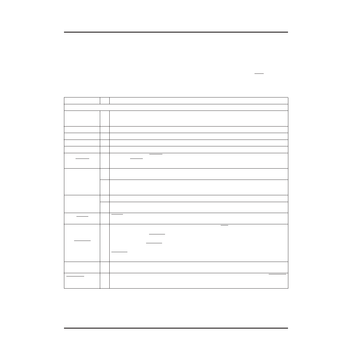
Table 15. Pin Descriptions
Symbol
I/O
Description
Dedicated Pins
VDD33
—
3.3 V positive power supply. This power supply is used for 3.3 V conguration RAMs and internal
PLLs. When using PLLs, this power supply should be well isolated from all other power supplies on
the board for proper operation.
VDD15
—
1.5 V positive power supply for internal logic.
VDDIO
—
Positive power supply used by I/O banks.
VSS
—
Ground.
PTEMP
I
Temperature sensing diode pin. Dedicated input.
RESET
I
During conguration, RESET forces the restart of conguration and a pull-up is enabled. After con-
guration, RESET can be used as a general FPGA input or as a direct input, which causes all PLC
latches/Flip-Flops to be asynchronously set/reset.
CCLK
O
In the master and asynchronous peripheral modes, CCLK is an output which strobes conguration
data in.
I
In the slave or readback after conguration, CCLK is input synchronous with the data on DIN or
D[7:0]. CCLK is an output for daisy-chain operation when the lead device is in master, peripheral, or
system bus modes.
DONE
I
As an input, a low level on DONE delays FPGA start-up after conguration.*
O
As an active-high, open-drain output, a high level on this signal indicates that conguration is com-
plete. DONE has an optional pull-up resistor.
PRGM
I
PRGM
is an active-low input that forces the restart of conguration and resets the boundary-scan
circuitry. This pin always has an active pull-up.
RD_CFG
I
This pin must be held high during device initialization until the INIT pin goes high. This pin always
has an active pull-up.
During conguration, RD_CFG is an active-low input that activates the TS_ALL function and 3-states
all of the I/O.
After conguration, RD_CFG can be selected (via a bit stream option) to activate the TS_ALL func-
tion as described above, or, if readback is enabled via a bit stream option, a high-to-low transition on
RD_CFG
will initiate readback of the conguration data, including PFU output states, starting with
frame address 0.
RD_DATA/TDO
O
RD_DATA/TDO is a dual-function pin. If used for readback, RD_DATA provides conguration data
out. If used in boundary-scan, TDO is test data out.
CFG_IRQ/MPI_IR
Q
O
During JTAG, slave, master, and asynchronous peripheral conguration, assertion on this CFG_IRQ
(active-low) indicates an error or errors for block RAM or FPSC initialization.
MPI active-low interrupt
request output, when the MPI is used.
*The timing of DONE release is controlled by one set of bit stream options, and the timing of the simultaneous release of all
other conguration pins (and the activation of all user I/Os) is controlled by a second set of options.
相关PDF资料 |
PDF描述 |
|---|---|
| ORLI10G2BM680-DB | FPGA, 1296 CLBS, 333000 GATES, PBGA680 |
| ORLI10G3BM680-DB | FPGA, 1296 CLBS, 333000 GATES, PBGA680 |
| ORT82G5-1BM680 | FPGA, 1296 CLBS, 380000 GATES, PBGA680 |
| ORT82G5-2BM680 | FPGA, 1296 CLBS, 380000 GATES, PBGA680 |
| ORT82G5-3BM680 | FPGA, 1296 CLBS, 380000 GATES, PBGA680 |
相关代理商/技术参数 |
参数描述 |
|---|---|
| ORLI10G-1BM680I | 功能描述:FPGA - 现场可编程门阵列 10368 LUT 316 I/O RoHS:否 制造商:Altera Corporation 系列:Cyclone V E 栅极数量: 逻辑块数量:943 内嵌式块RAM - EBR:1956 kbit 输入/输出端数量:128 最大工作频率:800 MHz 工作电源电压:1.1 V 最大工作温度:+ 70 C 安装风格:SMD/SMT 封装 / 箱体:FBGA-256 |
| ORLI10G-1BMN680C | 功能描述:FPGA - 现场可编程门阵列 10368 LUT 316 I/O RoHS:否 制造商:Altera Corporation 系列:Cyclone V E 栅极数量: 逻辑块数量:943 内嵌式块RAM - EBR:1956 kbit 输入/输出端数量:128 最大工作频率:800 MHz 工作电源电压:1.1 V 最大工作温度:+ 70 C 安装风格:SMD/SMT 封装 / 箱体:FBGA-256 |
| ORLI10G-1BMN680I | 功能描述:FPGA - 现场可编程门阵列 10368 LUT 316 I/O RoHS:否 制造商:Altera Corporation 系列:Cyclone V E 栅极数量: 逻辑块数量:943 内嵌式块RAM - EBR:1956 kbit 输入/输出端数量:128 最大工作频率:800 MHz 工作电源电压:1.1 V 最大工作温度:+ 70 C 安装风格:SMD/SMT 封装 / 箱体:FBGA-256 |
| ORLI10G-2BM680C | 功能描述:FPGA - 现场可编程门阵列 10368 LUT 316 I/O RoHS:否 制造商:Altera Corporation 系列:Cyclone V E 栅极数量: 逻辑块数量:943 内嵌式块RAM - EBR:1956 kbit 输入/输出端数量:128 最大工作频率:800 MHz 工作电源电压:1.1 V 最大工作温度:+ 70 C 安装风格:SMD/SMT 封装 / 箱体:FBGA-256 |
| ORLI10G-2BM680I | 功能描述:FPGA - 现场可编程门阵列 10368 LUT 316 I/O RoHS:否 制造商:Altera Corporation 系列:Cyclone V E 栅极数量: 逻辑块数量:943 内嵌式块RAM - EBR:1956 kbit 输入/输出端数量:128 最大工作频率:800 MHz 工作电源电压:1.1 V 最大工作温度:+ 70 C 安装风格:SMD/SMT 封装 / 箱体:FBGA-256 |
发布紧急采购,3分钟左右您将得到回复。