- 您现在的位置:买卖IC网 > PDF目录299581 > ORLI10G1BM680-DB (LATTICE SEMICONDUCTOR CORP) FPGA, 1296 CLBS, 333000 GATES, PBGA680 PDF资料下载
参数资料
| 型号: | ORLI10G1BM680-DB |
| 厂商: | LATTICE SEMICONDUCTOR CORP |
| 元件分类: | FPGA |
| 英文描述: | FPGA, 1296 CLBS, 333000 GATES, PBGA680 |
| 封装: | PLASTIC, FBGA-680 |
| 文件页数: | 49/78页 |
| 文件大小: | 1689K |
| 代理商: | ORLI10G1BM680-DB |
第1页第2页第3页第4页第5页第6页第7页第8页第9页第10页第11页第12页第13页第14页第15页第16页第17页第18页第19页第20页第21页第22页第23页第24页第25页第26页第27页第28页第29页第30页第31页第32页第33页第34页第35页第36页第37页第38页第39页第40页第41页第42页第43页第44页第45页第46页第47页第48页当前第49页第50页第51页第52页第53页第54页第55页第56页第57页第58页第59页第60页第61页第62页第63页第64页第65页第66页第67页第68页第69页第70页第71页第72页第73页第74页第75页第76页第77页第78页
Lattice Semiconductor
ORCA ORLI10G Data Sheet
53
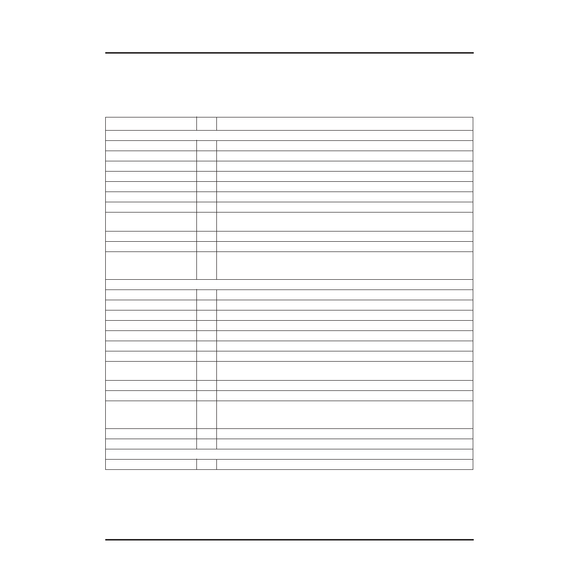
Pin Information (continued)
In Table 17, an output refers to a signal owing into the FGPA logic (out of the embedded core) and an input refers
to a signal owing out of the FPGA logic (into the embedded core).
Table 17. Embedded Core/FPGA Interface Signal Description
Symbol
I/O
Description
Receive Signals
RX_DAT_OUT<127:0>
O
Data from demultiplexer on receive side.
RX_CLK8_OUT<3:0>
O
Divided down clocks on receive side.
RX_ENB8_OUT<3:0>
O
Data enables on receive side.
RX1_VCOP
O
RX1_PLL output clock on receive side (M/N clock) after phase select.
RX1_VCO
O
RX1_PLL output clock on receive side (M/N clock) before phase select.
RX2_VCOP
O
RX2_PLL output clock on receive side (x1 clock) before phase select.
RX2_VCO
O
RX2_PLL output clock on receive side (x1 clock) before phase select.
RX2_FBCKI
I
PLL feedback input to RX2_PLL. This allows for the removal of the FPGA clock
routing delay.
RX1_BYPASS
I
Set to 1 to bypass the RX1 PLL.
RX2_BYPASS
I
Set to 1 to bypass the RX2 PLL
RX_LOCK
O
Lock the signal for RX1_PLL and RX2_PLL. This signal is a logical OR of the
lock signal from both PLLs. It is not integrated; thus, small glitches can occur
on this signal during normal PLL operation.
Transmit Signals
TX_DAT_IN<127:0>
I
Data to multiplexer on transmit side.
TX_CLK8_IN<3:0>
I
Clocks to multiplexer on transmit side.
TX_ENB8_IN<3:0>
I
Data enables on transmit side.
TX1_VCOP
O
TX1_PLL output clock on transmit side (M/N clock) after phase select.
TX1_VCO
O
TX1_PLL output clock on transmit side (M/N clock) before phase select.
TX2_VCOP
O
TX2_PLL output clock on transmit side (x1 clock) after phase select.
TX2_VCO
O
TX2_PLL output clock on transmit side (x1 clock) before phase select.
TX2_FBCKI
I
PLL feedback input to TX2 PLL. This allows for the removal of the FPGA clock
routing delay.
TX1_BYPASS
I
Set to 1 to bypass the TX1 PLL.
TX2_BYPASS
I
Set to 1 to bypass the TX2 PLL.
TX_LOCK
O
Lock signal for TX1_PLL and TX2_PLL. This signal is a logical OR of the lock
signal from both PLLs. It is not integrated; thus, small glitches can occur on
this signal during normal operation.
VSS_A<7:4>
—
Analog ground for the embedded line interface PLLs.
VDD33_A<7:4>
—
Analog power supply for the embedded line interface PLLs.
Miscellaneous Signals
FPGA_RESET
I
A logic 1 resets all receive and transmit logic, including PLLs.
相关PDF资料 |
PDF描述 |
|---|---|
| ORLI10G2BM680-DB | FPGA, 1296 CLBS, 333000 GATES, PBGA680 |
| ORLI10G3BM680-DB | FPGA, 1296 CLBS, 333000 GATES, PBGA680 |
| ORT82G5-1BM680 | FPGA, 1296 CLBS, 380000 GATES, PBGA680 |
| ORT82G5-2BM680 | FPGA, 1296 CLBS, 380000 GATES, PBGA680 |
| ORT82G5-3BM680 | FPGA, 1296 CLBS, 380000 GATES, PBGA680 |
相关代理商/技术参数 |
参数描述 |
|---|---|
| ORLI10G-1BM680I | 功能描述:FPGA - 现场可编程门阵列 10368 LUT 316 I/O RoHS:否 制造商:Altera Corporation 系列:Cyclone V E 栅极数量: 逻辑块数量:943 内嵌式块RAM - EBR:1956 kbit 输入/输出端数量:128 最大工作频率:800 MHz 工作电源电压:1.1 V 最大工作温度:+ 70 C 安装风格:SMD/SMT 封装 / 箱体:FBGA-256 |
| ORLI10G-1BMN680C | 功能描述:FPGA - 现场可编程门阵列 10368 LUT 316 I/O RoHS:否 制造商:Altera Corporation 系列:Cyclone V E 栅极数量: 逻辑块数量:943 内嵌式块RAM - EBR:1956 kbit 输入/输出端数量:128 最大工作频率:800 MHz 工作电源电压:1.1 V 最大工作温度:+ 70 C 安装风格:SMD/SMT 封装 / 箱体:FBGA-256 |
| ORLI10G-1BMN680I | 功能描述:FPGA - 现场可编程门阵列 10368 LUT 316 I/O RoHS:否 制造商:Altera Corporation 系列:Cyclone V E 栅极数量: 逻辑块数量:943 内嵌式块RAM - EBR:1956 kbit 输入/输出端数量:128 最大工作频率:800 MHz 工作电源电压:1.1 V 最大工作温度:+ 70 C 安装风格:SMD/SMT 封装 / 箱体:FBGA-256 |
| ORLI10G-2BM680C | 功能描述:FPGA - 现场可编程门阵列 10368 LUT 316 I/O RoHS:否 制造商:Altera Corporation 系列:Cyclone V E 栅极数量: 逻辑块数量:943 内嵌式块RAM - EBR:1956 kbit 输入/输出端数量:128 最大工作频率:800 MHz 工作电源电压:1.1 V 最大工作温度:+ 70 C 安装风格:SMD/SMT 封装 / 箱体:FBGA-256 |
| ORLI10G-2BM680I | 功能描述:FPGA - 现场可编程门阵列 10368 LUT 316 I/O RoHS:否 制造商:Altera Corporation 系列:Cyclone V E 栅极数量: 逻辑块数量:943 内嵌式块RAM - EBR:1956 kbit 输入/输出端数量:128 最大工作频率:800 MHz 工作电源电压:1.1 V 最大工作温度:+ 70 C 安装风格:SMD/SMT 封装 / 箱体:FBGA-256 |
发布紧急采购,3分钟左右您将得到回复。