- 您现在的位置:买卖IC网 > PDF目录299581 > ORLI10G1BM680-DB (LATTICE SEMICONDUCTOR CORP) FPGA, 1296 CLBS, 333000 GATES, PBGA680 PDF资料下载
参数资料
| 型号: | ORLI10G1BM680-DB |
| 厂商: | LATTICE SEMICONDUCTOR CORP |
| 元件分类: | FPGA |
| 英文描述: | FPGA, 1296 CLBS, 333000 GATES, PBGA680 |
| 封装: | PLASTIC, FBGA-680 |
| 文件页数: | 41/78页 |
| 文件大小: | 1689K |
| 代理商: | ORLI10G1BM680-DB |
第1页第2页第3页第4页第5页第6页第7页第8页第9页第10页第11页第12页第13页第14页第15页第16页第17页第18页第19页第20页第21页第22页第23页第24页第25页第26页第27页第28页第29页第30页第31页第32页第33页第34页第35页第36页第37页第38页第39页第40页当前第41页第42页第43页第44页第45页第46页第47页第48页第49页第50页第51页第52页第53页第54页第55页第56页第57页第58页第59页第60页第61页第62页第63页第64页第65页第66页第67页第68页第69页第70页第71页第72页第73页第74页第75页第76页第77页第78页
Lattice Semiconductor
ORCA ORLI10G Data Sheet
46
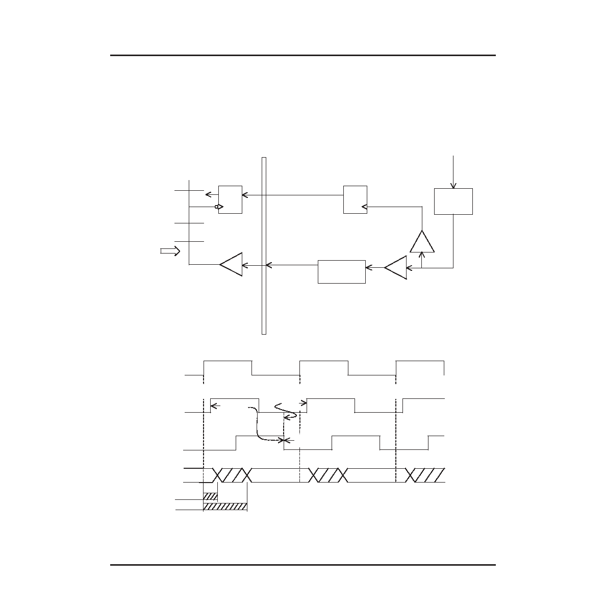
Figure 32 shows the Receive (Embedded Line Interface to FPGA) timing for 10G mode where PLL_RX2 is
bypassed via the PLL_BYPASS external FPSC pin. The 0.7 ns minimum propagation delay and 1.9 ns maximum
propagation delay shown are approximate values for the embedded line interface in this scenario. In the waveform
shown, data will be time shifted at the FPGA capture register due to FPGA data path delay. Consult the ispLEVER
software, via the static timing analysis tool TRACE, for the exact timing values. Figure 32 shows a half cycle trans-
fer; note the inversion bubble on the FPGA capture register. This half cycle transfer negates possible hold timing
issues. If a full cycle transfer is used with the receive PLL bypassed, check for hold violations with the static timing
analysis tool TRACE.
Figure 32. Receive Timing for 10G Mode with PLL Bypassed (-1 Speed Grade)
1.9 ns Tpd_max
3.0ns
0.7 ns Tpd_min
Launch
RX_CLK8_IN_MUX1
1.4ns
3ns
RX_DAT_IN
Primary
FPGA Clock
Tree
Clock
Divider
PLL_RX2
(Bypass Mode)
D
RX2_VCOP
Embedded Line Interface Core
FPGA
Q
RX_CLK_IN[0]
(100 MHz)
0.0ns
5.0ns
10.0ns
15.0ns
20.0ns
RX2_VCOP
(Reference Clock)
5.6ns
15.6ns
RX_CLK8_IN_MUX1
13.0ns
18.0ns
FPGA Clock
Data
0.6ns
10.6ns
20.6ns
Hold
0.8ns
Capture
8.0ns
相关PDF资料 |
PDF描述 |
|---|---|
| ORLI10G2BM680-DB | FPGA, 1296 CLBS, 333000 GATES, PBGA680 |
| ORLI10G3BM680-DB | FPGA, 1296 CLBS, 333000 GATES, PBGA680 |
| ORT82G5-1BM680 | FPGA, 1296 CLBS, 380000 GATES, PBGA680 |
| ORT82G5-2BM680 | FPGA, 1296 CLBS, 380000 GATES, PBGA680 |
| ORT82G5-3BM680 | FPGA, 1296 CLBS, 380000 GATES, PBGA680 |
相关代理商/技术参数 |
参数描述 |
|---|---|
| ORLI10G-1BM680I | 功能描述:FPGA - 现场可编程门阵列 10368 LUT 316 I/O RoHS:否 制造商:Altera Corporation 系列:Cyclone V E 栅极数量: 逻辑块数量:943 内嵌式块RAM - EBR:1956 kbit 输入/输出端数量:128 最大工作频率:800 MHz 工作电源电压:1.1 V 最大工作温度:+ 70 C 安装风格:SMD/SMT 封装 / 箱体:FBGA-256 |
| ORLI10G-1BMN680C | 功能描述:FPGA - 现场可编程门阵列 10368 LUT 316 I/O RoHS:否 制造商:Altera Corporation 系列:Cyclone V E 栅极数量: 逻辑块数量:943 内嵌式块RAM - EBR:1956 kbit 输入/输出端数量:128 最大工作频率:800 MHz 工作电源电压:1.1 V 最大工作温度:+ 70 C 安装风格:SMD/SMT 封装 / 箱体:FBGA-256 |
| ORLI10G-1BMN680I | 功能描述:FPGA - 现场可编程门阵列 10368 LUT 316 I/O RoHS:否 制造商:Altera Corporation 系列:Cyclone V E 栅极数量: 逻辑块数量:943 内嵌式块RAM - EBR:1956 kbit 输入/输出端数量:128 最大工作频率:800 MHz 工作电源电压:1.1 V 最大工作温度:+ 70 C 安装风格:SMD/SMT 封装 / 箱体:FBGA-256 |
| ORLI10G-2BM680C | 功能描述:FPGA - 现场可编程门阵列 10368 LUT 316 I/O RoHS:否 制造商:Altera Corporation 系列:Cyclone V E 栅极数量: 逻辑块数量:943 内嵌式块RAM - EBR:1956 kbit 输入/输出端数量:128 最大工作频率:800 MHz 工作电源电压:1.1 V 最大工作温度:+ 70 C 安装风格:SMD/SMT 封装 / 箱体:FBGA-256 |
| ORLI10G-2BM680I | 功能描述:FPGA - 现场可编程门阵列 10368 LUT 316 I/O RoHS:否 制造商:Altera Corporation 系列:Cyclone V E 栅极数量: 逻辑块数量:943 内嵌式块RAM - EBR:1956 kbit 输入/输出端数量:128 最大工作频率:800 MHz 工作电源电压:1.1 V 最大工作温度:+ 70 C 安装风格:SMD/SMT 封装 / 箱体:FBGA-256 |
发布紧急采购,3分钟左右您将得到回复。