- 您现在的位置:买卖IC网 > PDF目录299581 > ORLI10G1BM680-DB (LATTICE SEMICONDUCTOR CORP) FPGA, 1296 CLBS, 333000 GATES, PBGA680 PDF资料下载
参数资料
| 型号: | ORLI10G1BM680-DB |
| 厂商: | LATTICE SEMICONDUCTOR CORP |
| 元件分类: | FPGA |
| 英文描述: | FPGA, 1296 CLBS, 333000 GATES, PBGA680 |
| 封装: | PLASTIC, FBGA-680 |
| 文件页数: | 50/78页 |
| 文件大小: | 1689K |
| 代理商: | ORLI10G1BM680-DB |
第1页第2页第3页第4页第5页第6页第7页第8页第9页第10页第11页第12页第13页第14页第15页第16页第17页第18页第19页第20页第21页第22页第23页第24页第25页第26页第27页第28页第29页第30页第31页第32页第33页第34页第35页第36页第37页第38页第39页第40页第41页第42页第43页第44页第45页第46页第47页第48页第49页当前第50页第51页第52页第53页第54页第55页第56页第57页第58页第59页第60页第61页第62页第63页第64页第65页第66页第67页第68页第69页第70页第71页第72页第73页第74页第75页第76页第77页第78页
Lattice Semiconductor
ORCA ORLI10G Data Sheet
54
Package Pinouts
Table 18 provides the number of user-programmable I/Os available for each available package. Table 19 provides
the package pin and pin function for the ORLI10G FPSC and packages. The bond pad name is identied in the PIO
nomenclature used in the ispLEVER design editor. The bank column provides information as to which output volt-
age level bank the given pin is in. The group column provides information as to the group of pins the given pin is in.
This is used to show which VREF pin is used to provide the reference voltage for single-ended limited-swing I/Os. If
none of these buffer types (such as SSTL, GTL, HSTL) are used in a given group, then the VREF pin is available as
an I/O pin.
When the number of FPGA bond pads exceeds the number of package pins, bond pads are unused. When the
number of package pins exceeds the number of bond pads, package pins are left unconnected (no connects).
When a package pin is to be left as a no connect for a specic die, it is indicated as a note in the device column for
the FPGA. The tables provide no information on unused pads.
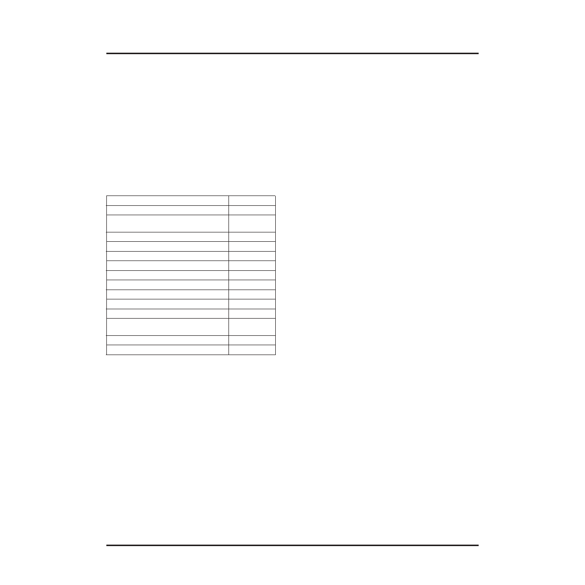
Table 18. ORCA Programmable I/Os Summary
The built-in MicroProcessor Interface (MPI) cannot be fully utilized in the 680-pin PBGA package because the
implementation of the XGMII interface limits the number of available address and data pins.
As shown in the Pair columns in Table 19, differential pairs and physical locations are numbered within each bank
(e.g., L19C_A0 is the nineteenth pair in an associated bank). A C indicates complementary differential, whereas a
T indicates true differential. An _A0 indicates the physical location of adjacent balls in either the horizontal or verti-
cal direction. Other physical indicators are as follows:
_A1 indicates one ball between pairs.
_A2 indicates two balls between pairs.
_D0 indicates balls are diagonally adjacent.
_D1 indicates balls are diagonally adjacent separated by one physical ball.
VREF pins, shown in the Pin Description column in Table 19, are associated to the bank and group
(e.g., VREF_TL_01 is the VREF for group one of the Top Left (TL) bank).
Device
680 PBGAM
User programmable I/O
316
Available programmable differential pair
pins
272
FPGA conguration pins
7
FPGA dedicated function pins
2
Core function pins
86
VDD15
86
VDD33_A
4
VDD33
28
VDDIO
44
VSS
95
VSS_A
4
LVCTAP for dedicated differential chan-
nels
6
Core LV_REF pins
4
Total package pins
680
相关PDF资料 |
PDF描述 |
|---|---|
| ORLI10G2BM680-DB | FPGA, 1296 CLBS, 333000 GATES, PBGA680 |
| ORLI10G3BM680-DB | FPGA, 1296 CLBS, 333000 GATES, PBGA680 |
| ORT82G5-1BM680 | FPGA, 1296 CLBS, 380000 GATES, PBGA680 |
| ORT82G5-2BM680 | FPGA, 1296 CLBS, 380000 GATES, PBGA680 |
| ORT82G5-3BM680 | FPGA, 1296 CLBS, 380000 GATES, PBGA680 |
相关代理商/技术参数 |
参数描述 |
|---|---|
| ORLI10G-1BM680I | 功能描述:FPGA - 现场可编程门阵列 10368 LUT 316 I/O RoHS:否 制造商:Altera Corporation 系列:Cyclone V E 栅极数量: 逻辑块数量:943 内嵌式块RAM - EBR:1956 kbit 输入/输出端数量:128 最大工作频率:800 MHz 工作电源电压:1.1 V 最大工作温度:+ 70 C 安装风格:SMD/SMT 封装 / 箱体:FBGA-256 |
| ORLI10G-1BMN680C | 功能描述:FPGA - 现场可编程门阵列 10368 LUT 316 I/O RoHS:否 制造商:Altera Corporation 系列:Cyclone V E 栅极数量: 逻辑块数量:943 内嵌式块RAM - EBR:1956 kbit 输入/输出端数量:128 最大工作频率:800 MHz 工作电源电压:1.1 V 最大工作温度:+ 70 C 安装风格:SMD/SMT 封装 / 箱体:FBGA-256 |
| ORLI10G-1BMN680I | 功能描述:FPGA - 现场可编程门阵列 10368 LUT 316 I/O RoHS:否 制造商:Altera Corporation 系列:Cyclone V E 栅极数量: 逻辑块数量:943 内嵌式块RAM - EBR:1956 kbit 输入/输出端数量:128 最大工作频率:800 MHz 工作电源电压:1.1 V 最大工作温度:+ 70 C 安装风格:SMD/SMT 封装 / 箱体:FBGA-256 |
| ORLI10G-2BM680C | 功能描述:FPGA - 现场可编程门阵列 10368 LUT 316 I/O RoHS:否 制造商:Altera Corporation 系列:Cyclone V E 栅极数量: 逻辑块数量:943 内嵌式块RAM - EBR:1956 kbit 输入/输出端数量:128 最大工作频率:800 MHz 工作电源电压:1.1 V 最大工作温度:+ 70 C 安装风格:SMD/SMT 封装 / 箱体:FBGA-256 |
| ORLI10G-2BM680I | 功能描述:FPGA - 现场可编程门阵列 10368 LUT 316 I/O RoHS:否 制造商:Altera Corporation 系列:Cyclone V E 栅极数量: 逻辑块数量:943 内嵌式块RAM - EBR:1956 kbit 输入/输出端数量:128 最大工作频率:800 MHz 工作电源电压:1.1 V 最大工作温度:+ 70 C 安装风格:SMD/SMT 封装 / 箱体:FBGA-256 |
发布紧急采购,3分钟左右您将得到回复。