- 您现在的位置:买卖IC网 > PDF目录299581 > ORLI10G1BM680-DB (LATTICE SEMICONDUCTOR CORP) FPGA, 1296 CLBS, 333000 GATES, PBGA680 PDF资料下载
参数资料
| 型号: | ORLI10G1BM680-DB |
| 厂商: | LATTICE SEMICONDUCTOR CORP |
| 元件分类: | FPGA |
| 英文描述: | FPGA, 1296 CLBS, 333000 GATES, PBGA680 |
| 封装: | PLASTIC, FBGA-680 |
| 文件页数: | 24/78页 |
| 文件大小: | 1689K |
| 代理商: | ORLI10G1BM680-DB |
第1页第2页第3页第4页第5页第6页第7页第8页第9页第10页第11页第12页第13页第14页第15页第16页第17页第18页第19页第20页第21页第22页第23页当前第24页第25页第26页第27页第28页第29页第30页第31页第32页第33页第34页第35页第36页第37页第38页第39页第40页第41页第42页第43页第44页第45页第46页第47页第48页第49页第50页第51页第52页第53页第54页第55页第56页第57页第58页第59页第60页第61页第62页第63页第64页第65页第66页第67页第68页第69页第70页第71页第72页第73页第74页第75页第76页第77页第78页
Lattice Semiconductor
ORCA ORLI10G Data Sheet
30
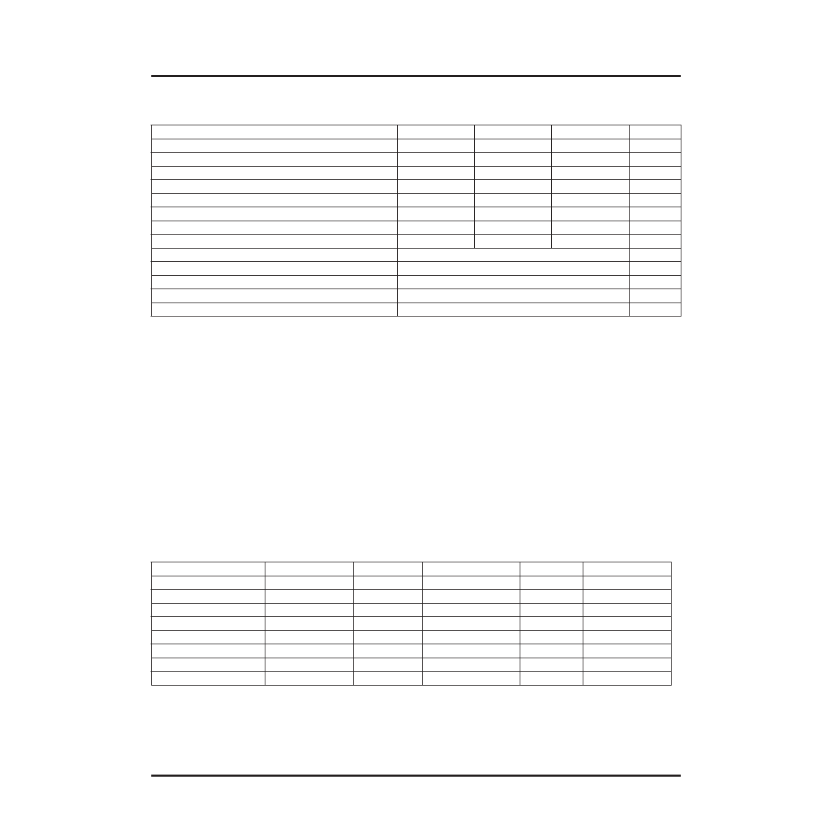
ORLI10G Embedded Programmable PLLs Specications
Table 2. Programmable PLL Specications
Notes:
Multiplication and division values can both be used on one PLL output (example 3/4x).
For more information about the HPPLL, see the Series 4 PLL Application Note.
ORLI10G Reset Requirements
Both the embedded core portion and the FPGA portion are reset at powerup. The embedded core is also reset, as
shown in Table 3, based on other conditions. All resets to the core can either be asynchronous or asynchronous on
with a synchronous release. Asynchronous resets must be held in reset for at least 8 ns. Two signals from the
FPGA logic can also reset the embedded core: the global set/reset (GSRN) which can be inhibited, and a signal
routed from the FPGA general routing (FPGA_RESET). Both of these affect both the TX and RX reset simulta-
neously. Table 3 also shows the conditions upon which the I/O are 3-stated.
Reset of PLL blocks directly affects only the digital logic. For the PLL_RX2 and PLL_TX2 (x1) PLLs, the VCO out-
puts from the PLL should be in the 3-6Mhz range during reset. For PLL_RX1 and PLL_TX1 (xM/N) PLLs using the
M and N counters, the VCO will go to the low state. Coming out of reset will require about 25 microseconds for the
PLLs to become stable.
Table 3. ORLI10G Reset Requirements
Parameters
Min
Nom
Max
Unit
VDD15
1.425
1.5
1.575
V
VDD33
3.0
3.3
3.6
V
Operating Temperature (TA)
–40
—
125
C
Input Clock Frequency
60
—
420
MHz
Input Duty Cycle
30
—
70
%
Output Clock Frequency
7.5
—
420
MHz
Output Duty Cycle
45
50
55
%
Lock Time
—
<50
—
s
Frequency Multiplication (TX1_PLL and RX1_PLL)
2x, 3x, 4x, 5x, 6x, 7x, 8x
—
Frequency Division (TX1_PLL and RX1_PLL)
1/8x, 1/7x, 1/6x, 1/5x, 1/4x, 1/3x, 1/2x
—
Duty Cycle Adjust of Output Clock(s)
12.5, 25, 37.5, 50, 62.5, 75, 87.5
%
Delay Adjust of Output Clock
0, 45, 90, 135, 180, 225, 270, 315
degrees
Phase Shift Between VCO and VCOP
0, 45, 90, 135, 180, 225, 270, 315
degrees
Condition
TX MUX Block
TX PLL
RX DeMUX Block
RX PLL
Embedded I/O
Powerup
Reset
3-state
FPGA Conguration
Reset
Active
FPGA GSRN
Reset
Active
FPGA_RESET Signal
Reset
Active
TS_ALL Pin = 1
—
3-state
RESET_TX Pin = 1
Reset
—
Active
RESET_RX Pin = 1
—
Reset
Active
PWRON Pin = 1
—
Powerdown
—
Powerdown
Active
相关PDF资料 |
PDF描述 |
|---|---|
| ORLI10G2BM680-DB | FPGA, 1296 CLBS, 333000 GATES, PBGA680 |
| ORLI10G3BM680-DB | FPGA, 1296 CLBS, 333000 GATES, PBGA680 |
| ORT82G5-1BM680 | FPGA, 1296 CLBS, 380000 GATES, PBGA680 |
| ORT82G5-2BM680 | FPGA, 1296 CLBS, 380000 GATES, PBGA680 |
| ORT82G5-3BM680 | FPGA, 1296 CLBS, 380000 GATES, PBGA680 |
相关代理商/技术参数 |
参数描述 |
|---|---|
| ORLI10G-1BM680I | 功能描述:FPGA - 现场可编程门阵列 10368 LUT 316 I/O RoHS:否 制造商:Altera Corporation 系列:Cyclone V E 栅极数量: 逻辑块数量:943 内嵌式块RAM - EBR:1956 kbit 输入/输出端数量:128 最大工作频率:800 MHz 工作电源电压:1.1 V 最大工作温度:+ 70 C 安装风格:SMD/SMT 封装 / 箱体:FBGA-256 |
| ORLI10G-1BMN680C | 功能描述:FPGA - 现场可编程门阵列 10368 LUT 316 I/O RoHS:否 制造商:Altera Corporation 系列:Cyclone V E 栅极数量: 逻辑块数量:943 内嵌式块RAM - EBR:1956 kbit 输入/输出端数量:128 最大工作频率:800 MHz 工作电源电压:1.1 V 最大工作温度:+ 70 C 安装风格:SMD/SMT 封装 / 箱体:FBGA-256 |
| ORLI10G-1BMN680I | 功能描述:FPGA - 现场可编程门阵列 10368 LUT 316 I/O RoHS:否 制造商:Altera Corporation 系列:Cyclone V E 栅极数量: 逻辑块数量:943 内嵌式块RAM - EBR:1956 kbit 输入/输出端数量:128 最大工作频率:800 MHz 工作电源电压:1.1 V 最大工作温度:+ 70 C 安装风格:SMD/SMT 封装 / 箱体:FBGA-256 |
| ORLI10G-2BM680C | 功能描述:FPGA - 现场可编程门阵列 10368 LUT 316 I/O RoHS:否 制造商:Altera Corporation 系列:Cyclone V E 栅极数量: 逻辑块数量:943 内嵌式块RAM - EBR:1956 kbit 输入/输出端数量:128 最大工作频率:800 MHz 工作电源电压:1.1 V 最大工作温度:+ 70 C 安装风格:SMD/SMT 封装 / 箱体:FBGA-256 |
| ORLI10G-2BM680I | 功能描述:FPGA - 现场可编程门阵列 10368 LUT 316 I/O RoHS:否 制造商:Altera Corporation 系列:Cyclone V E 栅极数量: 逻辑块数量:943 内嵌式块RAM - EBR:1956 kbit 输入/输出端数量:128 最大工作频率:800 MHz 工作电源电压:1.1 V 最大工作温度:+ 70 C 安装风格:SMD/SMT 封装 / 箱体:FBGA-256 |
发布紧急采购,3分钟左右您将得到回复。