- 您现在的位置:买卖IC网 > PDF目录299581 > ORLI10G1BM680-DB (LATTICE SEMICONDUCTOR CORP) FPGA, 1296 CLBS, 333000 GATES, PBGA680 PDF资料下载
参数资料
| 型号: | ORLI10G1BM680-DB |
| 厂商: | LATTICE SEMICONDUCTOR CORP |
| 元件分类: | FPGA |
| 英文描述: | FPGA, 1296 CLBS, 333000 GATES, PBGA680 |
| 封装: | PLASTIC, FBGA-680 |
| 文件页数: | 74/78页 |
| 文件大小: | 1689K |
| 代理商: | ORLI10G1BM680-DB |
第1页第2页第3页第4页第5页第6页第7页第8页第9页第10页第11页第12页第13页第14页第15页第16页第17页第18页第19页第20页第21页第22页第23页第24页第25页第26页第27页第28页第29页第30页第31页第32页第33页第34页第35页第36页第37页第38页第39页第40页第41页第42页第43页第44页第45页第46页第47页第48页第49页第50页第51页第52页第53页第54页第55页第56页第57页第58页第59页第60页第61页第62页第63页第64页第65页第66页第67页第68页第69页第70页第71页第72页第73页当前第74页第75页第76页第77页第78页
Lattice Semiconductor
ORCA ORLI10G Data Sheet
76
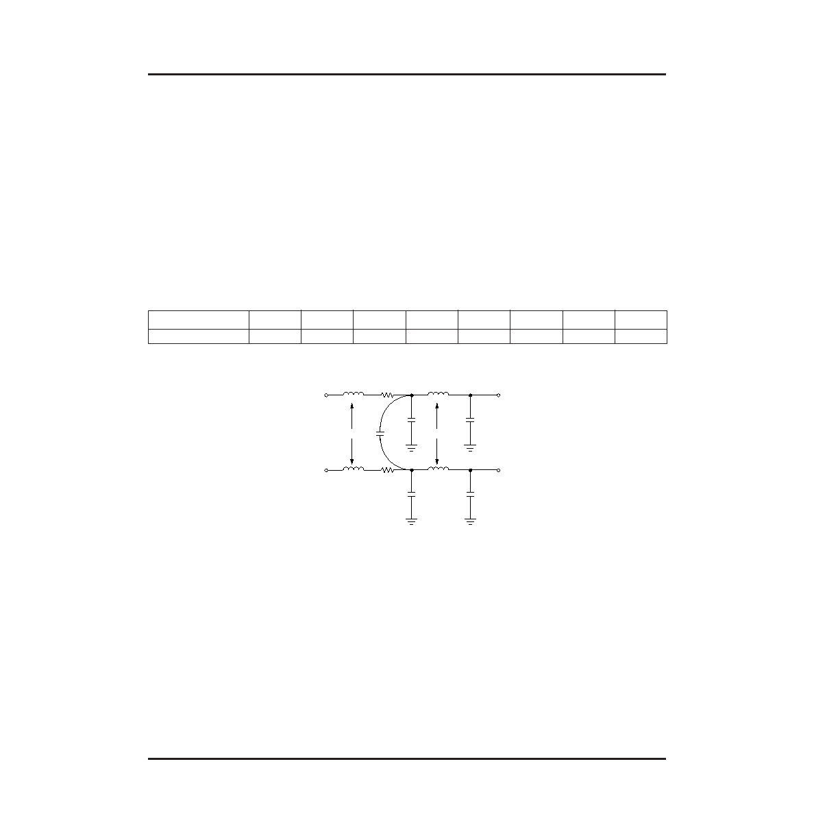
Package Parasitics
The electrical performance of an IC package, such as signal quality and noise sensitivity, is directly affected by the
package parasitics. Table 22 lists eight parasitics associated with the ORCA packages. These parasitics represent
the contributions of all components of a package, which include the bond wires, all internal package routing, and
the external leads.
Four inductances in nH are listed: LSW and LSL, the self-inductance of the lead; and LMW and LML, the mutual
inductance to the nearest neighbor lead. These parameters are important in determining ground bounce noise and
inductive crosstalk noise. Three capacitances in pF are listed: CM, the mutual capacitance of the lead to the near-
est neighbor lead; and C1 and C2, the total capacitance of the lead to all other leads (all other leads are assumed
to be grounded). These parameters are important in determining capacitive crosstalk and the capacitive loading
effect of the lead. Resistance values are in m.
The parasitic values in Table 22 are for the circuit model of bond wire and package lead parasitics. If the mutual
capacitance value is not used in the designer's model, then the value listed as mutual capacitance should be
added to each of the C1 and C2 capacitors.
Table 22. ORCA ORLI10G Package Parasitics
Figure 34. Package Parasitics
Package Outline Diagrams
Terms and Denitions
Basic Size (BSC): The basic size of a dimension is the size from which the limits for that dimension are derived by
the application of the allowance and the tolerance.
Design Size: The design size of a dimension is the actual size of the design, including an allowance for t and toler-
ance.
Typical (TYP): When specied after a dimension, this indicates the repeated design size if a tolerance is specied
or repeated basic size if a tolerance is not specied.
Reference (REF): The reference dimension is an untoleranced dimension used for informational purposes only. It is
a repeated dimension or one that can be derived from other values in the drawing.
Minimum (MIN) or Maximum (MAX): Indicates the minimum or maximum allowable size of a dimension.
Package Type
LSW
LMW
RW
C1
C2
CM
LSL
LML
680-Pin PBGAM
3.80
1.30
250
0.50
1.0
0.30
2.8—5.0
0.5—1.50
PAD N
LSW
RW
CIRCUIT
BOARD PAD
CM
C1
LSW
RW
LSL
LMW
C2
C1
LML
C2
LSL
PAD N + 1
相关PDF资料 |
PDF描述 |
|---|---|
| ORLI10G2BM680-DB | FPGA, 1296 CLBS, 333000 GATES, PBGA680 |
| ORLI10G3BM680-DB | FPGA, 1296 CLBS, 333000 GATES, PBGA680 |
| ORT82G5-1BM680 | FPGA, 1296 CLBS, 380000 GATES, PBGA680 |
| ORT82G5-2BM680 | FPGA, 1296 CLBS, 380000 GATES, PBGA680 |
| ORT82G5-3BM680 | FPGA, 1296 CLBS, 380000 GATES, PBGA680 |
相关代理商/技术参数 |
参数描述 |
|---|---|
| ORLI10G-1BM680I | 功能描述:FPGA - 现场可编程门阵列 10368 LUT 316 I/O RoHS:否 制造商:Altera Corporation 系列:Cyclone V E 栅极数量: 逻辑块数量:943 内嵌式块RAM - EBR:1956 kbit 输入/输出端数量:128 最大工作频率:800 MHz 工作电源电压:1.1 V 最大工作温度:+ 70 C 安装风格:SMD/SMT 封装 / 箱体:FBGA-256 |
| ORLI10G-1BMN680C | 功能描述:FPGA - 现场可编程门阵列 10368 LUT 316 I/O RoHS:否 制造商:Altera Corporation 系列:Cyclone V E 栅极数量: 逻辑块数量:943 内嵌式块RAM - EBR:1956 kbit 输入/输出端数量:128 最大工作频率:800 MHz 工作电源电压:1.1 V 最大工作温度:+ 70 C 安装风格:SMD/SMT 封装 / 箱体:FBGA-256 |
| ORLI10G-1BMN680I | 功能描述:FPGA - 现场可编程门阵列 10368 LUT 316 I/O RoHS:否 制造商:Altera Corporation 系列:Cyclone V E 栅极数量: 逻辑块数量:943 内嵌式块RAM - EBR:1956 kbit 输入/输出端数量:128 最大工作频率:800 MHz 工作电源电压:1.1 V 最大工作温度:+ 70 C 安装风格:SMD/SMT 封装 / 箱体:FBGA-256 |
| ORLI10G-2BM680C | 功能描述:FPGA - 现场可编程门阵列 10368 LUT 316 I/O RoHS:否 制造商:Altera Corporation 系列:Cyclone V E 栅极数量: 逻辑块数量:943 内嵌式块RAM - EBR:1956 kbit 输入/输出端数量:128 最大工作频率:800 MHz 工作电源电压:1.1 V 最大工作温度:+ 70 C 安装风格:SMD/SMT 封装 / 箱体:FBGA-256 |
| ORLI10G-2BM680I | 功能描述:FPGA - 现场可编程门阵列 10368 LUT 316 I/O RoHS:否 制造商:Altera Corporation 系列:Cyclone V E 栅极数量: 逻辑块数量:943 内嵌式块RAM - EBR:1956 kbit 输入/输出端数量:128 最大工作频率:800 MHz 工作电源电压:1.1 V 最大工作温度:+ 70 C 安装风格:SMD/SMT 封装 / 箱体:FBGA-256 |
发布紧急采购,3分钟左右您将得到回复。