- 您现在的位置:买卖IC网 > PDF目录1958 > ORT8850L-3BM680C (Lattice Semiconductor Corporation)IC FPSC TRANSCEIVER 8CH 680-BGA PDF资料下载
参数资料
| 型号: | ORT8850L-3BM680C |
| 厂商: | Lattice Semiconductor Corporation |
| 文件页数: | 31/105页 |
| 文件大小: | 0K |
| 描述: | IC FPSC TRANSCEIVER 8CH 680-BGA |
| 产品变化通告: | Product Discontinuation 01/Aug/2011 |
| 标准包装: | 24 |
| 系列: | * |
第1页第2页第3页第4页第5页第6页第7页第8页第9页第10页第11页第12页第13页第14页第15页第16页第17页第18页第19页第20页第21页第22页第23页第24页第25页第26页第27页第28页第29页第30页当前第31页第32页第33页第34页第35页第36页第37页第38页第39页第40页第41页第42页第43页第44页第45页第46页第47页第48页第49页第50页第51页第52页第53页第54页第55页第56页第57页第58页第59页第60页第61页第62页第63页第64页第65页第66页第67页第68页第69页第70页第71页第72页第73页第74页第75页第76页第77页第78页第79页第80页第81页第82页第83页第84页第85页第86页第87页第88页第89页第90页第91页第92页第93页第94页第95页第96页第97页第98页第99页第100页第101页第102页第103页第104页第105页
Lattice Semiconductor
ORCA ORT8850 Data Sheet
31
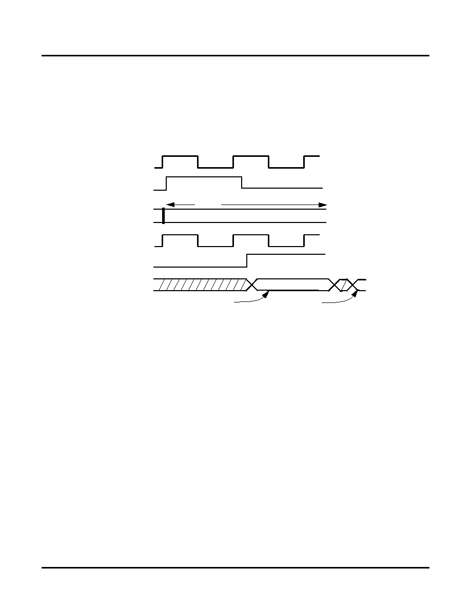
Serial TOH Insertion Mode
In the transmit direction the SPE bytes are always transferred unaltered from the input parallel bus to the serial
LVDS output. On the other hand, TOH bytes are received from the serial input port and are inserted in the STS-12
frame before being sent to the LVDS output in the Serial TOH Insertion mode. The FPGA logic must provide fram-
ing information to the Core using the TX_TOH_CK_EN Input signal. TOH data is input on a row by row basis, with a
one clock cycle frame pulse delineating the start of a row, as shown in Figure 14. As shown in the gure, while the
SPE bytes are being transmitted for one row, the FPGA logic must simultaneously supply the Core with the TOH
data for the next row. Detailed timing for the TOH serial input is shown later in Figure 31.
Figure 14. TOH Serial Port Input Framing Signals (FPGA to Core)
Incoming serial TOH data is synchronized initially to the free running clock, TOH_CLK. TOH_CLK can operate from
a minimum frequency of 25 Mhz. to a maximum frequency of 106 MHz. TOH bytes are transferred in the order
shown in Figure 15. Bytes are transferred over the serial links with the MSB rst. Data should be transferred over
the serial link on a row-by-row basis. With three TOH bytes/per row for each STS-1 stream and a total of 12 STS-1
streams per STS-12 frame, a total of 288 TOH bits must be transferred for each row. The 288 TOH bits per row can
be sent back-to-back. In this case, TX_TO_CLK_EN will be high continuously for 288 TOH_CLK cycles.
It is the responsibility of the user to synchronize transfer of the TOH bytes to a pre-determined window of time rela-
tive to the STS-12 frame position on the parallel input bus, i.e., the 36 TOH bytes to be inserted in row number n
must be transferred to the Core during the time the SPE bytes of row n-1 are being transferred to the Core over the
parallel input bus. Within each SPE row, a guard band of four TOH_CLK cycles must be provided on each side of
the TOH transfer window. No data may be transferred in these guard bands.
FPGA_SYSCLK
SYS_FP
DINxx[7:0]
TOH_CLK
TX_TOH_CK_EN
Row 1
TOH_INxx
36 bytes TOH
bit 6
of B1 byte STS1 #1
MSbit(7)
of B1 byte STS1 #1
相关PDF资料 |
PDF描述 |
|---|---|
| P1010PSE5HFA | MPU PROTO 800/667 425-TEPBGA1 |
| P1013NXN2LFB | IC MPU 1067MHZ 689TEPBGA |
| P1013PSE2EFA | IC MPU PROTO 600MHZ 689-TEPBGA |
| P1014NSN5DFA | IC MPU 800MHZ 425TEPBGA1 |
| P1014NSN5FFA | IC MPU 800MHZ 425TEPBGA1 |
相关代理商/技术参数 |
参数描述 |
|---|---|
| ORT8850L-3BMN680C | 功能描述:FPGA - 现场可编程门阵列 4992 LUT 278 I/O RoHS:否 制造商:Altera Corporation 系列:Cyclone V E 栅极数量: 逻辑块数量:943 内嵌式块RAM - EBR:1956 kbit 输入/输出端数量:128 最大工作频率:800 MHz 工作电源电压:1.1 V 最大工作温度:+ 70 C 安装风格:SMD/SMT 封装 / 箱体:FBGA-256 |
| ORT9303 | 制造商:BOT 制造商全称:Bedford Opto Technology Ltd. 功能描述:3 ELEMENT PCB MOUNT 1.8mm LED ARRAY |
| ORT9303B | 制造商:BOT 制造商全称:Bedford Opto Technology Ltd. 功能描述:3 ELEMENT PCB MOUNT 1.8mm LED ARRAY |
| ORT9303BL | 制造商:BOT 制造商全称:Bedford Opto Technology Ltd. 功能描述:3 ELEMENT PCB MOUNT 1.8mm LED ARRAY |
| ORT9303G | 制造商:BOT 制造商全称:Bedford Opto Technology Ltd. 功能描述:3 ELEMENT PCB MOUNT 1.8mm LED ARRAY |
发布紧急采购,3分钟左右您将得到回复。