- 您现在的位置:买卖IC网 > PDF目录1958 > ORT8850L-3BM680C (Lattice Semiconductor Corporation)IC FPSC TRANSCEIVER 8CH 680-BGA PDF资料下载
参数资料
| 型号: | ORT8850L-3BM680C |
| 厂商: | Lattice Semiconductor Corporation |
| 文件页数: | 47/105页 |
| 文件大小: | 0K |
| 描述: | IC FPSC TRANSCEIVER 8CH 680-BGA |
| 产品变化通告: | Product Discontinuation 01/Aug/2011 |
| 标准包装: | 24 |
| 系列: | * |
第1页第2页第3页第4页第5页第6页第7页第8页第9页第10页第11页第12页第13页第14页第15页第16页第17页第18页第19页第20页第21页第22页第23页第24页第25页第26页第27页第28页第29页第30页第31页第32页第33页第34页第35页第36页第37页第38页第39页第40页第41页第42页第43页第44页第45页第46页当前第47页第48页第49页第50页第51页第52页第53页第54页第55页第56页第57页第58页第59页第60页第61页第62页第63页第64页第65页第66页第67页第68页第69页第70页第71页第72页第73页第74页第75页第76页第77页第78页第79页第80页第81页第82页第83页第84页第85页第86页第87页第88页第89页第90页第91页第92页第93页第94页第95页第96页第97页第98页第99页第100页第101页第102页第103页第104页第105页
Lattice Semiconductor
ORCA ORT8850 Data Sheet
46
phases (i.e., received and system) are determined. This latch point is then stable unless the relative framing
changes and the received H byte times collide with the system F1 or E2 times, in which case the latch point would
be switched to the collision-free byte time.
There is no restriction on how many or how often increments and decrements are processed. Any received incre-
ment or decrement is immediately passed to the generator for implementation regardless of when the last pointer
adjustment was made. The responsibility for meeting the SONET criteria for maximum frequency of pointer adjust-
ments is left to an upstream pointer processor.
Receive Bypass Options
Not all of the blocks in the receive direction are required to be used. The following bypass options are valid in the
receive (backplane
→ FPGA) direction:
STM Pointer Mover bypass:
– In this mode, data from the alignment FIFOs is transferred to the FPGA logic. All channels are synchronous
to the FPGA_SYSCLK signals driven to the FPGA logic, as is also the case when the pointer mover is not
bypassed. During bypass SPE, C1J1, and data parity signals are not valid. When the pointer mover is
bypassed, eight frame pulses (DOUTxx_FP) from aligned channels are provided by the embedded core to
the FPGA.
– When the pointer mover is used, the FPGA logic provides the frame pulse on the LINE_FP (recall: there is
only one LINE_FP just like there is only one SYS_FP) signal essential for the Pointer Mover to move the
data. The FPGA gets eight channels of SONET data with the A1 byte position of each channel of the TOH
arbitrarily offset from the LINE_FP. The DOUTxx_FP signals are not valid when the pointer mover is used.
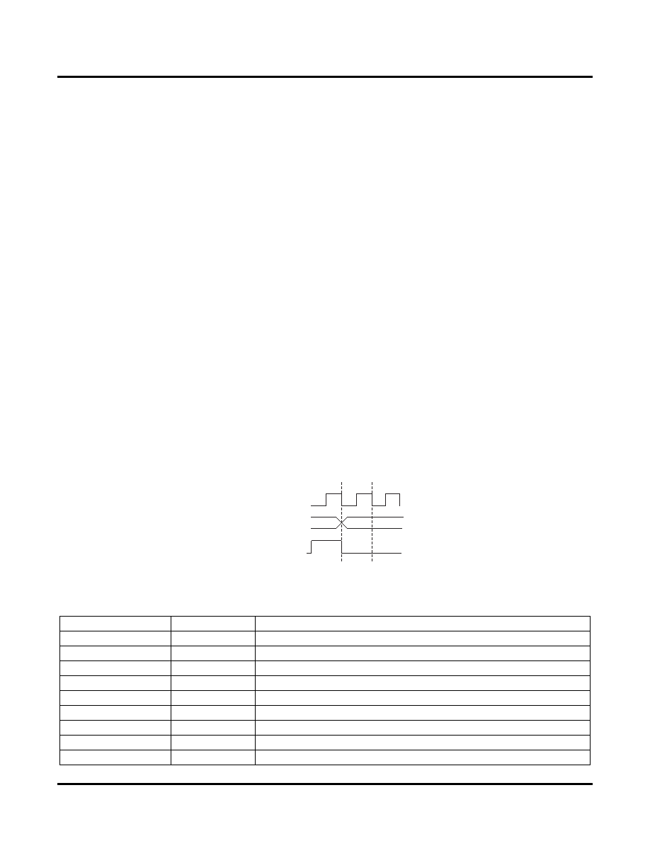
STM Pointer Mover and Alignment FIFO bypass:
– In this mode, data from the framer block is transferred to the FPGA logic. All channels supply data and frame
pulses synchronous with their individual recovered clock (CDR_CLK_xx) per channel. During bypass, SPE,
C1J1, and data parity signals are not valid. Additionally, no serial TOH_OUT_xx data and frame pulse sig-
nals will be available. The DOUTxx_FP signals are aligned with the A1 byte position of each channel, as
shown in Figure 26.
Figure 26. Pointer Mover and Alignment FIFO Bypass Timing
Table 14 shows the register settings to enable the bypass modes.
Table 14. Register Settings for Bypass Mode
Register Address
Value
Description
0x3000C
0x04
Turn off the SONET scrambler/descrambler
0x30020
0x07
Channel AA in functional mode
0x30038
0x07
Channel AB in functional mode
0x30050
0x07
Channel AC in functional mode
0x30068
0x07
Channel AD in functional mode
0x30080
0x07
Channel BA in functional mode
0x30098
0x07
Channel BB in functional mode
0x300B0
0x07
Channel BC in functional mode
0x300C8
0x07
Channel BD in functional mode
CDR_CLK_xx
DOUTxx
DOUTxx_FP
First A1 Byte
相关PDF资料 |
PDF描述 |
|---|---|
| P1010PSE5HFA | MPU PROTO 800/667 425-TEPBGA1 |
| P1013NXN2LFB | IC MPU 1067MHZ 689TEPBGA |
| P1013PSE2EFA | IC MPU PROTO 600MHZ 689-TEPBGA |
| P1014NSN5DFA | IC MPU 800MHZ 425TEPBGA1 |
| P1014NSN5FFA | IC MPU 800MHZ 425TEPBGA1 |
相关代理商/技术参数 |
参数描述 |
|---|---|
| ORT8850L-3BMN680C | 功能描述:FPGA - 现场可编程门阵列 4992 LUT 278 I/O RoHS:否 制造商:Altera Corporation 系列:Cyclone V E 栅极数量: 逻辑块数量:943 内嵌式块RAM - EBR:1956 kbit 输入/输出端数量:128 最大工作频率:800 MHz 工作电源电压:1.1 V 最大工作温度:+ 70 C 安装风格:SMD/SMT 封装 / 箱体:FBGA-256 |
| ORT9303 | 制造商:BOT 制造商全称:Bedford Opto Technology Ltd. 功能描述:3 ELEMENT PCB MOUNT 1.8mm LED ARRAY |
| ORT9303B | 制造商:BOT 制造商全称:Bedford Opto Technology Ltd. 功能描述:3 ELEMENT PCB MOUNT 1.8mm LED ARRAY |
| ORT9303BL | 制造商:BOT 制造商全称:Bedford Opto Technology Ltd. 功能描述:3 ELEMENT PCB MOUNT 1.8mm LED ARRAY |
| ORT9303G | 制造商:BOT 制造商全称:Bedford Opto Technology Ltd. 功能描述:3 ELEMENT PCB MOUNT 1.8mm LED ARRAY |
发布紧急采购,3分钟左右您将得到回复。