- 您现在的位置:买卖IC网 > PDF目录225140 > S29CD032G0RFFN003 (SPANSION LLC) 1M X 32 FLASH 2.7V PROM, 48 ns, PBGA80 PDF资料下载
参数资料
| 型号: | S29CD032G0RFFN003 |
| 厂商: | SPANSION LLC |
| 元件分类: | PROM |
| 英文描述: | 1M X 32 FLASH 2.7V PROM, 48 ns, PBGA80 |
| 封装: | 13 X 11 MM, 1 MM PITCH, LEAD FREE, FORTIFIED, BGA-80 |
| 文件页数: | 25/81页 |
| 文件大小: | 1276K |
| 代理商: | S29CD032G0RFFN003 |
第1页第2页第3页第4页第5页第6页第7页第8页第9页第10页第11页第12页第13页第14页第15页第16页第17页第18页第19页第20页第21页第22页第23页第24页当前第25页第26页第27页第28页第29页第30页第31页第32页第33页第34页第35页第36页第37页第38页第39页第40页第41页第42页第43页第44页第45页第46页第47页第48页第49页第50页第51页第52页第53页第54页第55页第56页第57页第58页第59页第60页第61页第62页第63页第64页第65页第66页第67页第68页第69页第70页第71页第72页第73页第74页第75页第76页第77页第78页第79页第80页第81页
March 3, 2009 S29CD-G_00_B1
S29CD-G Flash Family
29
Da ta
Shee t
(Prelim i nar y )
12.11.6
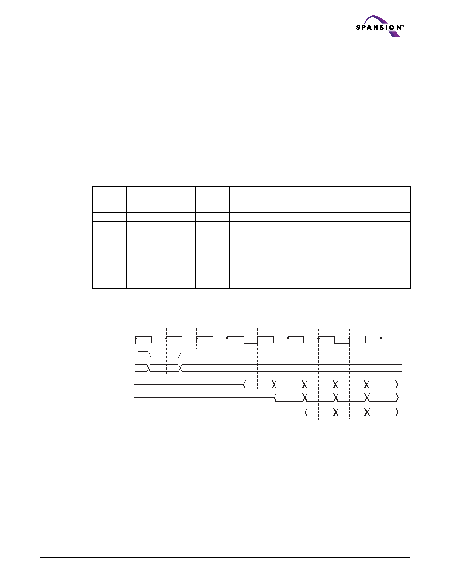
Burst Access Timing Control
In addition to the IND/WAIT# signal control, burst controls exist in the Control Register for initial access delay,
delivery of data on the CLK edge, and the length of time data is held.
12.11.7
Initial Burst Access Delay Control
The device contains options for initial access delay of a burst access. The initial access delay has no effect on
asynchronous read operations.
Burst Initial Access Delay is defined as the number of clock cycles that must elapse from the first valid clock
edge after ADV# assertion (or the rising edge of ADV#) until the first valid CLK edge when the data is valid.
The burst access is initiated and the address is latched on the first rising CLK edge when ADV# is active or
upon a rising ADV# edge, whichever comes first. (Table 12.6 describes the initial access delay
configurations.)
Figure 12.3 Initial Burst Delay Control
Notes
1. Burst access starts with a rising CLK edge and when ADV# is active.
2. Configurations register 6 is always set to 1 (CR6 = 1). Burst starts and data outputs on the rising CLK edge.
3. CR [13-10] = 1 or three clock cycles
4. CR [13-10] = 2 or four clock cycles
5. CR [13-10] = 3 or five clock cycles
12.11.8
Burst CLK Edge Data Delivery
The device delivers data on the rising of CLK. Bit 6 in the Control Register (CR6) is set to 1, and is the default
configuration.
Table 12.6 Burst Initial Access Delay
CR13
CR12
CR11
CR10
Initial Burst Access (CLK cycles)
40 MHz (0J), 56 MHz (0M), 66 MHz (0P),
75 MHz (0R, 32 Mb only)
0000
2
0001
3
0010
4
0011
5
0100
6
0101
7
0
110
8
0111
9
CLK
ADV#
Addresses
DQ31-DQ03
DQ31-DQ04
DQ31-DQ05
Valid Address
Three CLK Delay
2nd CLK
3rd CLK
4th CLK
5th CLK
1st CLK
Four CLK Delay
Address 1 Latched
Five CLK Delay
D0
D1
D2
D3
D0
D1
D2
D0
D1
D2
D3
D4
相关PDF资料 |
PDF描述 |
|---|---|
| S29CD032G0RQFI012 | 1M X 32 FLASH 2.7V PROM, 48 ns, PQFP80 |
| S29CL032J0JFAM020 | 1M X 32 FLASH 3.3V PROM, 54 ns, PBGA80 |
| S29CL032J0JFFM020 | 1M X 32 FLASH 3.3V PROM, 54 ns, PBGA80 |
| S29CL032J0RFAM012 | 1M X 32 FLASH 3.3V PROM, 48 ns, PBGA80 |
| S29GL032A10TAIR11 | Ceramic Chip Capacitors / High Voltage; Capacitance [nom]: 3.3pF; Working Voltage (Vdc)[max]: 500V; Capacitance Tolerance: +/-10%; Dielectric: Multilayer Ceramic; Temperature Coefficient: C0G (NP0); Lead Style: Surface Mount Chip; Lead Dimensions: 0805; Termination: Solder (SnPb) Plated Nickel Barrier; Body Dimensions: 0.079" x 0.049"; Container: Bulk; Features: High Voltage; Unmarked |
相关代理商/技术参数 |
参数描述 |
|---|---|
| S29CD032J0MQAN010 | 制造商:Spansion 功能描述: |
| S29CD032J0MQFM010U | 制造商:Spansion 功能描述:N/A - Trays |
| S29CD032J0PFAM010 | 制造商:Spansion 功能描述: |
| S29CD032J0PQFI010 | 制造商:Spansion 功能描述:AUTO 3.3V 512KX32 FLASH - Trays |
| S29CL016J0JQFM030 | 制造商:Spansion 功能描述:FLASH PARALLEL 3.3V 16MBIT 512KX32 54NS 80PQFP - Trays |
发布紧急采购,3分钟左右您将得到回复。