- 您现在的位置:买卖IC网 > PDF目录225140 > S29CD032G0RFFN003 (SPANSION LLC) 1M X 32 FLASH 2.7V PROM, 48 ns, PBGA80 PDF资料下载
参数资料
| 型号: | S29CD032G0RFFN003 |
| 厂商: | SPANSION LLC |
| 元件分类: | PROM |
| 英文描述: | 1M X 32 FLASH 2.7V PROM, 48 ns, PBGA80 |
| 封装: | 13 X 11 MM, 1 MM PITCH, LEAD FREE, FORTIFIED, BGA-80 |
| 文件页数: | 57/81页 |
| 文件大小: | 1276K |
| 代理商: | S29CD032G0RFFN003 |
第1页第2页第3页第4页第5页第6页第7页第8页第9页第10页第11页第12页第13页第14页第15页第16页第17页第18页第19页第20页第21页第22页第23页第24页第25页第26页第27页第28页第29页第30页第31页第32页第33页第34页第35页第36页第37页第38页第39页第40页第41页第42页第43页第44页第45页第46页第47页第48页第49页第50页第51页第52页第53页第54页第55页第56页当前第57页第58页第59页第60页第61页第62页第63页第64页第65页第66页第67页第68页第69页第70页第71页第72页第73页第74页第75页第76页第77页第78页第79页第80页第81页
58
S29CD-G Flash Family
S29CD-G_00_B1 March 3, 2009
Data
Sheet
(Pre limin ar y)
Under both these conditions, the system must issue the reset command to return the device to reading array
data.
16.7
DQ3: Sector Erase Timer
After writing a sector erase command sequence, the system may read DQ3 to determine whether or not an
erase operation started. (The sector erase timer does not apply to the chip erase command.) If additional
sectors are selected for erasure, the entire time-out also applies after each additional sector erase command.
When the time-out is complete, DQ3 switches from 0 to 1. The system may ignore DQ3 if the system can
guarantee that the time between additional sector erase commands is always less than 50 s. Also see
After the sector erase command sequence is written, the system should read the status on DQ7 (Data#
Polling) or DQ6 (Toggle Bit I) to ensure the device accepted the command sequence, and then read DQ3. If
DQ3 is 1, the internally controlled erase cycle started; all further commands (other than Erase Suspend) are
ignored until the erase operation is complete. If DQ3 is 0, the device accepts additional sector erase
commands. To ensure the command is accepted, the system software should check the status of DQ3 prior
to and following each subsequent sector erase command. If DQ3 is high on the second status check, the last
command might not have been accepted. Table 16.1 shows the outputs for DQ3.
Notes
1. DQ5 switches to 1 when an Embedded Program or Embedded Erase operation exceeds the maximum timing limits. See DQ5: Exceeded
Timing Limits on page 57 for more information.
2. DQ7 and DQ2 require a valid address when reading status information. See DQ7: Data# Polling on page 54 and DQ2: Toggle Bit II
on page 56 for further details.
17. Absolute Maximum Ratings
Notes
1. Minimum DC voltage on input or I/O pins is –0.5 V. During voltage transitions, input at I/O pins may overshoot VSS to -2.0V for periods of
up to 20 ns. See Figure 17.2 on page 59. Maximum DC voltage on output and I/O pins is 3.6V (16Mb), 2.75V (32Mb). During voltage
transitions output pins may overshoot to VCC + 2.0V for periods up to 20 ns. See Figure 17.2 on page 59.
2. Minimum DC input voltage on pins ACC, A9, OE#, and RESET# is -0.5 V. During voltage transitions, A9, OE#, and RESET# may
overshoot VSS to -2.0V for periods of up to 20 ns. See Figure 17.1 on page 59. Maximum DC input voltage on pin A9 and OE# is +13.0 V
which may overshoot to 14.0 V for periods up to 20 ns.
3. No more than one output may be shorted to ground at a time. Duration of the short circuit should not be greater than one second.
4. Stresses above those listed under Absolute Maximum Ratings may cause permanent damage to the device. This is a stress rating only;
functional operation of the device at these or any other conditions above those indicated in the operational sections of this data sheet is not
implied. Exposure of the device to absolute maximum rating conditions for extended periods may affect device reliability.
5. Parameter describes VIO power supply.
6. Parameter describes I/O pin voltage tolerances.
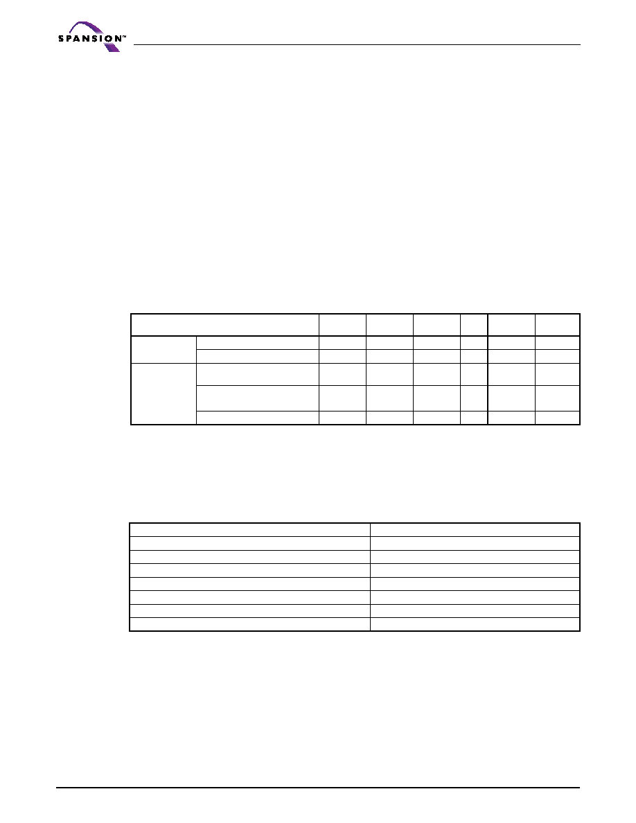
Table 16.1 Write Operation Status
Operation
DQ7
DQ6
DQ5
DQ3
DQ2
RY/BY#
Standard
Mode
Embedded Program Algorithm
DQ7#
Toggle
0
N/A
No toggle
0
Embedded Erase Algorithm
0
Toggle
0
1
Toggle
0
Erase
Suspend
Mode
Reading within Erase
Suspended Sector
1
No toggle
0
N/A
Toggle
1
Reading within Non-Erase
Suspended Sector
Data
1
Erase-Suspend-Program
DQ7#
Toggle
0
N/A
0
Storage Temperature, Plastic Packages
–65°C to +150°C
Ambient Temperature with Power Applied
–65°C to +145°C
-0.5 V to + 3.0V (16Mb), -0.5V to + 2.75V (32Mb)
ACC, A9, OE#, and RESET# (Note 2)
–0.5 V to +13.0 V
Address, Data, Control Signals
-0.5V to 3.6V (16 Mb), –0.5 V to 2.75 V (32 Mb)
All other pins (Notes 1, 6)
-0.5V to 3.6V (16 Mb),–0.5 V to 2.75 V (32 Mb)
Output Short Circuit Current (Note 3)
200 mA
相关PDF资料 |
PDF描述 |
|---|---|
| S29CD032G0RQFI012 | 1M X 32 FLASH 2.7V PROM, 48 ns, PQFP80 |
| S29CL032J0JFAM020 | 1M X 32 FLASH 3.3V PROM, 54 ns, PBGA80 |
| S29CL032J0JFFM020 | 1M X 32 FLASH 3.3V PROM, 54 ns, PBGA80 |
| S29CL032J0RFAM012 | 1M X 32 FLASH 3.3V PROM, 48 ns, PBGA80 |
| S29GL032A10TAIR11 | Ceramic Chip Capacitors / High Voltage; Capacitance [nom]: 3.3pF; Working Voltage (Vdc)[max]: 500V; Capacitance Tolerance: +/-10%; Dielectric: Multilayer Ceramic; Temperature Coefficient: C0G (NP0); Lead Style: Surface Mount Chip; Lead Dimensions: 0805; Termination: Solder (SnPb) Plated Nickel Barrier; Body Dimensions: 0.079" x 0.049"; Container: Bulk; Features: High Voltage; Unmarked |
相关代理商/技术参数 |
参数描述 |
|---|---|
| S29CD032J0MQAN010 | 制造商:Spansion 功能描述: |
| S29CD032J0MQFM010U | 制造商:Spansion 功能描述:N/A - Trays |
| S29CD032J0PFAM010 | 制造商:Spansion 功能描述: |
| S29CD032J0PQFI010 | 制造商:Spansion 功能描述:AUTO 3.3V 512KX32 FLASH - Trays |
| S29CL016J0JQFM030 | 制造商:Spansion 功能描述:FLASH PARALLEL 3.3V 16MBIT 512KX32 54NS 80PQFP - Trays |
发布紧急采购,3分钟左右您将得到回复。