- 您现在的位置:买卖IC网 > PDF目录11652 > AD9992BBCZ (Analog Devices Inc)IC CCD SGNL PROC 12BIT 105CSPBGA PDF资料下载
参数资料
| 型号: | AD9992BBCZ |
| 厂商: | Analog Devices Inc |
| 文件页数: | 22/92页 |
| 文件大小: | 0K |
| 描述: | IC CCD SGNL PROC 12BIT 105CSPBGA |
| 产品变化通告: | AD9992 Discontinuation 22/Feb/2012 |
| 标准包装: | 1 |
| 类型: | CCD 信号处理器,12 位 |
| 输入类型: | 逻辑 |
| 输出类型: | 逻辑 |
| 接口: | 3 线串口 |
| 电流 - 电源: | 27mA |
| 安装类型: | 表面贴装 |
| 封装/外壳: | 105-LFBGA,CSPBGA |
| 供应商设备封装: | 105-CSPBGA(8x8) |
| 包装: | 托盘 |
第1页第2页第3页第4页第5页第6页第7页第8页第9页第10页第11页第12页第13页第14页第15页第16页第17页第18页第19页第20页第21页当前第22页第23页第24页第25页第26页第27页第28页第29页第30页第31页第32页第33页第34页第35页第36页第37页第38页第39页第40页第41页第42页第43页第44页第45页第46页第47页第48页第49页第50页第51页第52页第53页第54页第55页第56页第57页第58页第59页第60页第61页第62页第63页第64页第65页第66页第67页第68页第69页第70页第71页第72页第73页第74页第75页第76页第77页第78页第79页第80页第81页第82页第83页第84页第85页第86页第87页第88页第89页第90页第91页第92页
AD9992
Rev. C | Page 29 of 92
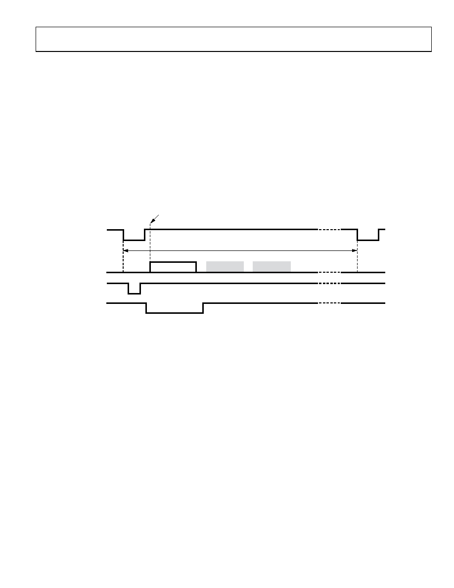
VERTICAL SEQUENCES (VSEQ)
The vertical sequences are created by selecting one of the V-pattern
groups and adding repeats, start position, horizontal clamping,
and blanking information. The V-sequences are programmed
the different registers are used to generate each V-sequence.
The VPATSELA, VPATSELB, VPATSELC, and VPATSELD
registers select which V-pattern is used in a given V-sequence.
Having four groups available allows different vertical outputs to
be mapped to different V-patterns. The selected V-pattern group
can have repetitions added for high speed line shifts or for line
binning by using the VREP registers for odd and even lines.
Generally, the same number of repetitions is programmed
into both registers. If a different number of repetitions is required
on odd and even lines, separate values can be used for each
register (see the Generating Line Alternation for V-Sequences
and HBLK section). The VSTARTA and VSTARTB registers
specify where in the line the V-pattern group starts. The
VMASK_EN register is used with the FREEZE/RESUME
registers to enable optional masking of the V-outputs. Either or
both of the FREEZE1/RESUME1 and FREEZE2/RESUME2
registers can be enabled.
The line length (in pixels) is programmable using the HDLEN
registers. Each V-sequence can have a different line length to
accommodate various image readout techniques. The maximum
number of pixels per line is 8192. The last line of the field is
programmed separately using the HDLASTLEN register, which
is located in the field register section.
VREP 3
HD
XV1 TO XV24
V-PATTERN GROUP
1
3
CLPOB
HBLK
2
44
VREP 2
5
6
PROGRAMMABLE SETTINGS FOR EACH VERTICAL SEQUENCE:
1START POSITION IN THE LINE OF SELECTED V-PATTERN GROUP.
2HD LINE LENGTH.
3V-PATTERN SELECT (VPATSEL) TO SELECT ANY V-PATTERN GROUP.
4NUMBER OF REPETITIONS OF THE V-PATTERN GROUP (IF NEEDED).
5START POLARITY AND TOGGLE POSITIONS FOR CLPOB AND PBLK SIGNALS.
6MASKING POLARITY AND TOGGLE POSITIONS FOR HBLK SIGNAL.
05
89
1
-03
5
Figure 35. V-Sequence Programmability
相关PDF资料 |
PDF描述 |
|---|---|
| VI-JN3-IY-F1 | CONVERTER MOD DC/DC 24V 50W |
| VI-JN2-IZ-B1 | CONVERTER MOD DC/DC 15V 25W |
| VI-JN2-IY-F4 | CONVERTER MOD DC/DC 15V 50W |
| VI-JN2-IY-F3 | CONVERTER MOD DC/DC 15V 50W |
| AD22050NZ | IC AMP DIFF SGL SUPPLY 8-DIP |
相关代理商/技术参数 |
参数描述 |
|---|---|
| AD9992BBCZRL | 功能描述:IC CCD SGNL PROC 12BIT 105CSPBGA RoHS:是 类别:集成电路 (IC) >> 接口 - 传感器和探测器接口 系列:- 其它有关文件:Automotive Product Guide 产品培训模块:Lead (SnPb) Finish for COTS Obsolescence Mitigation Program 标准包装:74 系列:- 类型:触控式传感器 输入类型:数字 输出类型:数字 接口:JTAG,串行 电流 - 电源:100µA 安装类型:表面贴装 封装/外壳:20-TSSOP(0.173",4.40mm 宽) 供应商设备封装:20-TSSOP 包装:管件 |
| AD9993BBCZ | 功能描述:IC MIXED-SIGNAL FRONT END 196BGA 制造商:analog devices inc. 系列:- 包装:托盘 零件状态:在售 类型:ADC,DAC 输入类型:LVDS 输出类型:LVDS 接口:SPI 电流 - 电源:- 工作温度:- 安装类型:表面贴装 封装/外壳:196-LFBGA,CSPBGA 供应商器件封装:196-CSPBGA(12x12) 标准包装:1 |
| AD9993BBCZRL | 功能描述:IC MIXED-SIGNAL FRONT END 196BGA 制造商:analog devices inc. 系列:- 包装:带卷(TR) 零件状态:在售 类型:ADC,DAC 输入类型:LVDS 输出类型:LVDS 接口:SPI 电流 - 电源:- 工作温度:- 安装类型:表面贴装 封装/外壳:196-LFBGA,CSPBGA 供应商器件封装:196-CSPBGA(12x12) 标准包装:1,500 |
| AD9993-EBZ | 功能描述:EVAL BOARD MXFE AD9993 制造商:analog devices inc. 系列:* 零件状态:在售 标准包装:1 |
| AD9994 | 制造商:AD 制造商全称:Analog Devices 功能描述:12-Bit CCD Signal Processor with Precision Timing Generator |
发布紧急采购,3分钟左右您将得到回复。