- 您现在的位置:买卖IC网 > PDF目录11652 > AD9992BBCZ (Analog Devices Inc)IC CCD SGNL PROC 12BIT 105CSPBGA PDF资料下载
参数资料
| 型号: | AD9992BBCZ |
| 厂商: | Analog Devices Inc |
| 文件页数: | 62/92页 |
| 文件大小: | 0K |
| 描述: | IC CCD SGNL PROC 12BIT 105CSPBGA |
| 产品变化通告: | AD9992 Discontinuation 22/Feb/2012 |
| 标准包装: | 1 |
| 类型: | CCD 信号处理器,12 位 |
| 输入类型: | 逻辑 |
| 输出类型: | 逻辑 |
| 接口: | 3 线串口 |
| 电流 - 电源: | 27mA |
| 安装类型: | 表面贴装 |
| 封装/外壳: | 105-LFBGA,CSPBGA |
| 供应商设备封装: | 105-CSPBGA(8x8) |
| 包装: | 托盘 |
第1页第2页第3页第4页第5页第6页第7页第8页第9页第10页第11页第12页第13页第14页第15页第16页第17页第18页第19页第20页第21页第22页第23页第24页第25页第26页第27页第28页第29页第30页第31页第32页第33页第34页第35页第36页第37页第38页第39页第40页第41页第42页第43页第44页第45页第46页第47页第48页第49页第50页第51页第52页第53页第54页第55页第56页第57页第58页第59页第60页第61页当前第62页第63页第64页第65页第66页第67页第68页第69页第70页第71页第72页第73页第74页第75页第76页第77页第78页第79页第80页第81页第82页第83页第84页第85页第86页第87页第88页第89页第90页第91页第92页
AD9992
Rev. C | Page 65 of 92
Table 26. Power-Up Register Write Sequence
Address
Data
Description
0x10
0x01
Resets all registers to default values
0x26
User-defined
Standby3 vertical output polarities
0x20 to
0xFFF
User-defined
Horizontal, vertical, shutter timing
0xD8
0x888
Configures start-up register
0x00
0x04
Powers up the AFE, enables OB clamp
0x15
0x01
Starts CLO oscillator (if using crystal)
0x14
0x01
Starts internal timing core
0x20
0x01
Configures for master mode
0x11
0x01
Enables all outputs after SYNC
0x13
0x4XX1
SWSYNC (if using software SYNC)
Using the SWSYNC Register
If an external SYNC pulse is not available, it is possible to
generate an internal SYNC in the AD9992 by writing 1 to the
SWSYNC register (Address 0x13, Bit 14). If the software SYNC
option is used, the SYNC input (Pin D3) should be low (VSS)
during power-up. The SYNCENABLE register (Address 0x13,
Bit 0) should be set high.
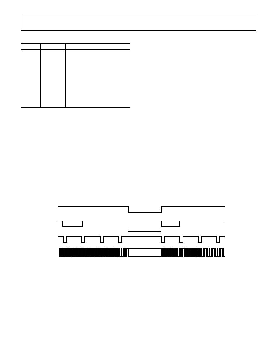
SYNC During Master Mode Operation
The hardware SYNC input can be used anytime during
operation to synchronize the AD9992 counters with external
timing, as shown in Figure 75. The operation of the digital
outputs can be suspended during the SYNC operation by set-
ting the SYNCSUSPEND register (Address 0x13, Bit 2) to 1. If
SYNCSUSPEND = 1, the polarities of the outputs are held at the
same state as OUTCONTROL = low, as shown in Table 27.
Power-Up and Synchronization in Slave Mode
The power-up procedure for slave mode operation is the same
as the procedure for master mode operation with two exceptions:
Eliminate Step 8. Do not write the part into master mode.
No SYNC pulse is required in slave mode. Substitute
Step 10 with starting the external VD and HD signals.
This synchronizes the part, allows the register updates,
and starts the timing operation.
When the AD9992 is used in slave mode, the VD/HD inputs are
used to synchronize the internal counters. After a falling edge of
VD, there is a latency of 36 master clock CLI edges after the falling
edge of HD until the internal H-counter is reset. The reset
operation is shown in Figure 76.
Additional Restrictions in Slave Mode
When operating in slave mode, the following restrictions
should be noted:
The HD falling edge should be located in the same CLI
clock cycle as the VD falling edge or later than the VD
falling edge. The HD falling edge should not be located
within five cycles prior to the VD falling edge.
If possible, all start-up serial writes should be performed
with VD and HD disabled. This prevents unknown
behavior caused by partial updating of registers before all
information is loaded.
VD
HD
SUSPEND
SYNC
H1 TO H4, RG,
XV1 TO XV24,
VSG, SUBCK
NOTES
1. THE SYNC RISING EDGE RESETS VD/HD AND COUNTERS TO 0.
2. SYNC POLARITY IS PROGRAMMABLE USING SYNCPOL REGISTER (ADDR 0x13).
3. DURING SYNC LOW, ALL INTERNAL COUNTERS ARE RESET AND VD/HD CAN BE SUSPENDED USING THE SYNCSUSPEND REGISTER (ADDR 0x13).
4. IF SYNCSUSPEND = 1, VERTICAL CLOCKS, H1 TO H4, AND RG ARE HELD AT THE SAME POLARITY SPECIFIED BY OUTCONTROL = LOW.
5. IF SYNCSUSPEND = 0, ALL CLOCK OUTPUTS CONTINUE TO OPERATE NORMALLY UNTIL THE SYNC RESET EDGE.
05
89
1-
0
70
Figure 75. SYNC Timing to Synchronize the AD9992 with External Timing
相关PDF资料 |
PDF描述 |
|---|---|
| VI-JN3-IY-F1 | CONVERTER MOD DC/DC 24V 50W |
| VI-JN2-IZ-B1 | CONVERTER MOD DC/DC 15V 25W |
| VI-JN2-IY-F4 | CONVERTER MOD DC/DC 15V 50W |
| VI-JN2-IY-F3 | CONVERTER MOD DC/DC 15V 50W |
| AD22050NZ | IC AMP DIFF SGL SUPPLY 8-DIP |
相关代理商/技术参数 |
参数描述 |
|---|---|
| AD9992BBCZRL | 功能描述:IC CCD SGNL PROC 12BIT 105CSPBGA RoHS:是 类别:集成电路 (IC) >> 接口 - 传感器和探测器接口 系列:- 其它有关文件:Automotive Product Guide 产品培训模块:Lead (SnPb) Finish for COTS Obsolescence Mitigation Program 标准包装:74 系列:- 类型:触控式传感器 输入类型:数字 输出类型:数字 接口:JTAG,串行 电流 - 电源:100µA 安装类型:表面贴装 封装/外壳:20-TSSOP(0.173",4.40mm 宽) 供应商设备封装:20-TSSOP 包装:管件 |
| AD9993BBCZ | 功能描述:IC MIXED-SIGNAL FRONT END 196BGA 制造商:analog devices inc. 系列:- 包装:托盘 零件状态:在售 类型:ADC,DAC 输入类型:LVDS 输出类型:LVDS 接口:SPI 电流 - 电源:- 工作温度:- 安装类型:表面贴装 封装/外壳:196-LFBGA,CSPBGA 供应商器件封装:196-CSPBGA(12x12) 标准包装:1 |
| AD9993BBCZRL | 功能描述:IC MIXED-SIGNAL FRONT END 196BGA 制造商:analog devices inc. 系列:- 包装:带卷(TR) 零件状态:在售 类型:ADC,DAC 输入类型:LVDS 输出类型:LVDS 接口:SPI 电流 - 电源:- 工作温度:- 安装类型:表面贴装 封装/外壳:196-LFBGA,CSPBGA 供应商器件封装:196-CSPBGA(12x12) 标准包装:1,500 |
| AD9993-EBZ | 功能描述:EVAL BOARD MXFE AD9993 制造商:analog devices inc. 系列:* 零件状态:在售 标准包装:1 |
| AD9994 | 制造商:AD 制造商全称:Analog Devices 功能描述:12-Bit CCD Signal Processor with Precision Timing Generator |
发布紧急采购,3分钟左右您将得到回复。