- 您现在的位置:买卖IC网 > PDF目录11652 > AD9992BBCZ (Analog Devices Inc)IC CCD SGNL PROC 12BIT 105CSPBGA PDF资料下载
参数资料
| 型号: | AD9992BBCZ |
| 厂商: | Analog Devices Inc |
| 文件页数: | 6/92页 |
| 文件大小: | 0K |
| 描述: | IC CCD SGNL PROC 12BIT 105CSPBGA |
| 产品变化通告: | AD9992 Discontinuation 22/Feb/2012 |
| 标准包装: | 1 |
| 类型: | CCD 信号处理器,12 位 |
| 输入类型: | 逻辑 |
| 输出类型: | 逻辑 |
| 接口: | 3 线串口 |
| 电流 - 电源: | 27mA |
| 安装类型: | 表面贴装 |
| 封装/外壳: | 105-LFBGA,CSPBGA |
| 供应商设备封装: | 105-CSPBGA(8x8) |
| 包装: | 托盘 |
第1页第2页第3页第4页第5页当前第6页第7页第8页第9页第10页第11页第12页第13页第14页第15页第16页第17页第18页第19页第20页第21页第22页第23页第24页第25页第26页第27页第28页第29页第30页第31页第32页第33页第34页第35页第36页第37页第38页第39页第40页第41页第42页第43页第44页第45页第46页第47页第48页第49页第50页第51页第52页第53页第54页第55页第56页第57页第58页第59页第60页第61页第62页第63页第64页第65页第66页第67页第68页第69页第70页第71页第72页第73页第74页第75页第76页第77页第78页第79页第80页第81页第82页第83页第84页第85页第86页第87页第88页第89页第90页第91页第92页
AD9992
Rev. C | Page 14 of 92
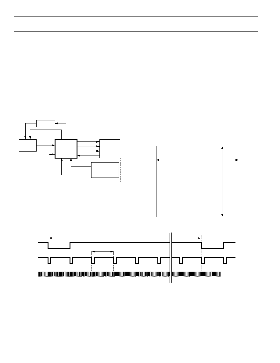
SYSTEM OVERVIEW
Figure 12 shows the typical system block diagram for the AD9992
in master mode. The CCD output is processed by AD9992 AFE
circuitry, which consists of a CDS, VGA, black level clamp, and
ADC. The digitized pixel information is sent to the digital
image processor chip, which performs the postprocessing and
compression. To operate the CCD, all CCD timing parameters
are programmed into the AD9992 from the system microprocessor
through the 3-wire serial interface. The AD9992 generates the
CCD’s horizontal and vertical clocks and internal AFE clocks
from the master clock, CLI, which is provided by the image
processor or external crystal,. External synchronization is provided
by a sync pulse from the microprocessor, which resets the
internal counters and resyncs the VD and HD outputs.
CCDIN
GPO1 TO GPO8
H1 TO H8, HL,
RG
XV1 TO XV24, XSUBCK
CCD
AD9992
AFETG
DIGITAL
IMAGE
PROCESSING
ASIC
DOUT
DCLK
HD, VD
CLI
SERIAL
INTERFACE
SYNC
MICROPROCESSOR
V-DRIVER
05
89
1-
01
2
Figure 12. Typical System Block Diagram, Master Mode
Alternatively, the AD9992 can operate in slave mode. In slave
mode, the VD and HD are provided externally from the image
processor, and all AD9992 timing synchronizes with VD and HD.
H-drivers for H1 to H8, HL, and RG are included in the AD9992,
allowing these clocks to be directly connected to the CCD.
An H-driver voltage of up to 3.3 V is supported. An external
V-driver is required for the vertical transfer clocks, the sensor
gate pulses, and the substrate clock.
The AD9992 includes programmable general-purpose outputs
(GPO), which can trigger mechanical shutter and strobe (flash)
circuitry.
vertical counter dimensions for the AD9992. All internal
horizontal and vertical clocking is controlled by these counters,
which specify line and pixel locations. Maximum HD length
is 8192 pixels per line; maximum VD length is 8192 lines per field.
13-BIT HORIZONTAL = 8192 PIXELS MAX
13-BIT VERTICAL = 8192 LINES MAX
MAXIMUM COUNTER DIMENSIONS
0
58
91
-01
3
Figure 13. Vertical and Horizontal Counters
VD
HD
MAX VD LENGTH IS 8192 LINES
CLI
MAX HD LENGTH IS 8192 PIXELS
0
589
1-
0
14
Figure 14. Maximum VD/HD Dimensions
相关PDF资料 |
PDF描述 |
|---|---|
| VI-JN3-IY-F1 | CONVERTER MOD DC/DC 24V 50W |
| VI-JN2-IZ-B1 | CONVERTER MOD DC/DC 15V 25W |
| VI-JN2-IY-F4 | CONVERTER MOD DC/DC 15V 50W |
| VI-JN2-IY-F3 | CONVERTER MOD DC/DC 15V 50W |
| AD22050NZ | IC AMP DIFF SGL SUPPLY 8-DIP |
相关代理商/技术参数 |
参数描述 |
|---|---|
| AD9992BBCZRL | 功能描述:IC CCD SGNL PROC 12BIT 105CSPBGA RoHS:是 类别:集成电路 (IC) >> 接口 - 传感器和探测器接口 系列:- 其它有关文件:Automotive Product Guide 产品培训模块:Lead (SnPb) Finish for COTS Obsolescence Mitigation Program 标准包装:74 系列:- 类型:触控式传感器 输入类型:数字 输出类型:数字 接口:JTAG,串行 电流 - 电源:100µA 安装类型:表面贴装 封装/外壳:20-TSSOP(0.173",4.40mm 宽) 供应商设备封装:20-TSSOP 包装:管件 |
| AD9993BBCZ | 功能描述:IC MIXED-SIGNAL FRONT END 196BGA 制造商:analog devices inc. 系列:- 包装:托盘 零件状态:在售 类型:ADC,DAC 输入类型:LVDS 输出类型:LVDS 接口:SPI 电流 - 电源:- 工作温度:- 安装类型:表面贴装 封装/外壳:196-LFBGA,CSPBGA 供应商器件封装:196-CSPBGA(12x12) 标准包装:1 |
| AD9993BBCZRL | 功能描述:IC MIXED-SIGNAL FRONT END 196BGA 制造商:analog devices inc. 系列:- 包装:带卷(TR) 零件状态:在售 类型:ADC,DAC 输入类型:LVDS 输出类型:LVDS 接口:SPI 电流 - 电源:- 工作温度:- 安装类型:表面贴装 封装/外壳:196-LFBGA,CSPBGA 供应商器件封装:196-CSPBGA(12x12) 标准包装:1,500 |
| AD9993-EBZ | 功能描述:EVAL BOARD MXFE AD9993 制造商:analog devices inc. 系列:* 零件状态:在售 标准包装:1 |
| AD9994 | 制造商:AD 制造商全称:Analog Devices 功能描述:12-Bit CCD Signal Processor with Precision Timing Generator |
发布紧急采购,3分钟左右您将得到回复。