- 您现在的位置:买卖IC网 > PDF目录11652 > AD9992BBCZ (Analog Devices Inc)IC CCD SGNL PROC 12BIT 105CSPBGA PDF资料下载
参数资料
| 型号: | AD9992BBCZ |
| 厂商: | Analog Devices Inc |
| 文件页数: | 26/92页 |
| 文件大小: | 0K |
| 描述: | IC CCD SGNL PROC 12BIT 105CSPBGA |
| 产品变化通告: | AD9992 Discontinuation 22/Feb/2012 |
| 标准包装: | 1 |
| 类型: | CCD 信号处理器,12 位 |
| 输入类型: | 逻辑 |
| 输出类型: | 逻辑 |
| 接口: | 3 线串口 |
| 电流 - 电源: | 27mA |
| 安装类型: | 表面贴装 |
| 封装/外壳: | 105-LFBGA,CSPBGA |
| 供应商设备封装: | 105-CSPBGA(8x8) |
| 包装: | 托盘 |
第1页第2页第3页第4页第5页第6页第7页第8页第9页第10页第11页第12页第13页第14页第15页第16页第17页第18页第19页第20页第21页第22页第23页第24页第25页当前第26页第27页第28页第29页第30页第31页第32页第33页第34页第35页第36页第37页第38页第39页第40页第41页第42页第43页第44页第45页第46页第47页第48页第49页第50页第51页第52页第53页第54页第55页第56页第57页第58页第59页第60页第61页第62页第63页第64页第65页第66页第67页第68页第69页第70页第71页第72页第73页第74页第75页第76页第77页第78页第79页第80页第81页第82页第83页第84页第85页第86页第87页第88页第89页第90页第91页第92页
AD9992
Rev. C | Page 32 of 92
XV1
XV8
HD
XV9
XV10
XV1 TO XV8 USE
V-PATTERN GROUP A
XV9, XV10 USE
V-PATTERN GROUP B
05
89
1-
03
6
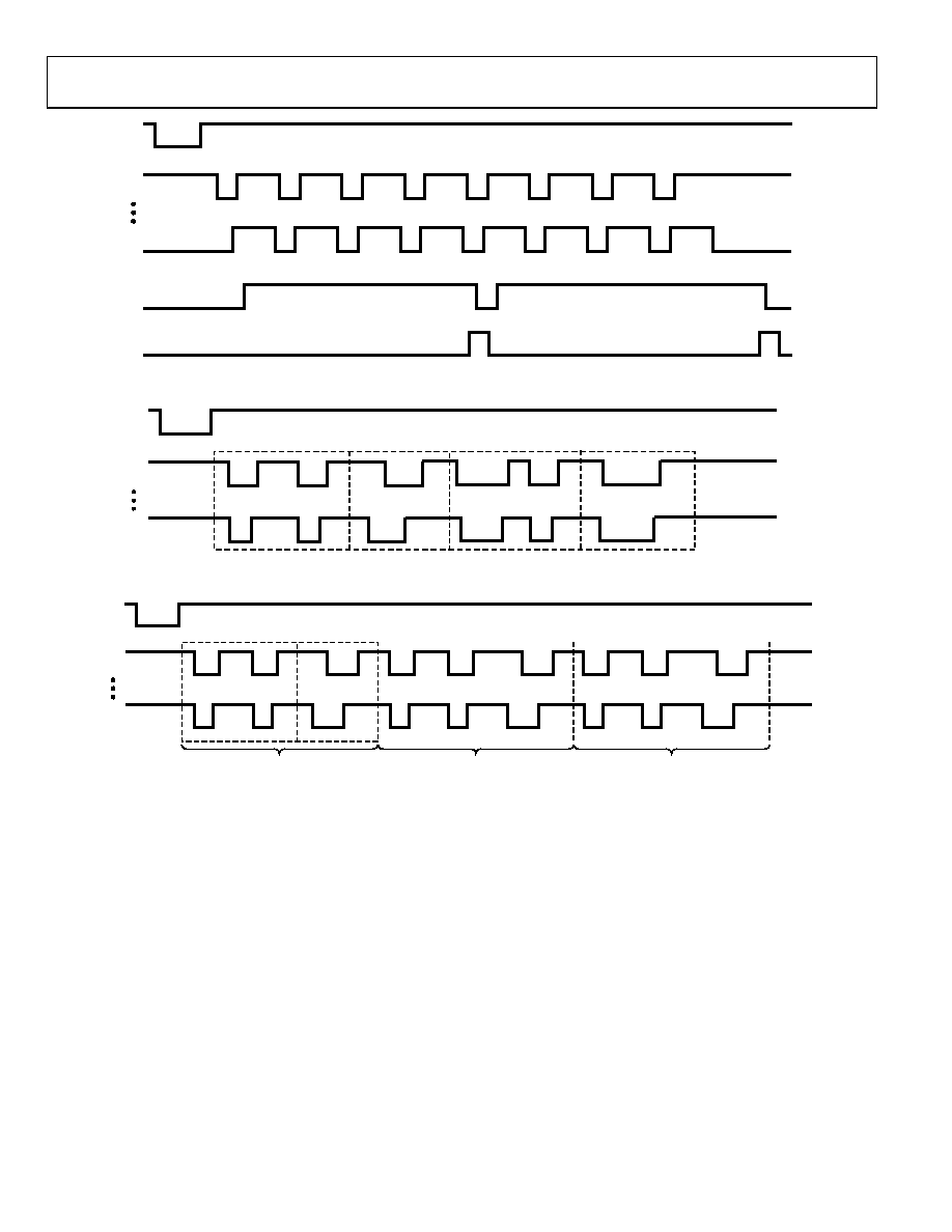
Figure 36. Using Separate Group A and Group B V-Patterns
XV1
XV24
HD
V-PATTERN GROUP A
V-PATTERN GROUP B
V-PATTERN GROUP C
V-PATTERN GROUP D
05
89
1-
0
37
Figure 37. Combining Multiple V-Patterns Using CONCAT_GRP = 1
XV1
XV10
HD
V-PATTERN GROUP A V-PATTERN GROUP B
GROUP A REP 1
GROUP A REP 2
GROUP A REP 3
05
89
1-
0
38
Figure 38. Combining Group A and Group B V-Patterns with Repetition
Group A/Group B/Group C/Group D Selection
The AD9992 has the flexibility to use four different V-pattern
groups in a vertical sequence. In general, the vertical outputs
use the same V-pattern group during a particular sequence. It is
possible to assign some of the outputs to a different V-pattern
group, which can be useful in certain CCD readout modes.
The GROUPSEL registers are used to select Group A, Group B,
Group C, or Group D for each V-output. In general, only a single
V-pattern group is needed for the vertical outputs; therefore,
Group A should be selected for all outputs by default
(GROUPSEL_0, GROUPSEL_1 = 0x00). In this configuration,
all outputs use the V-pattern group specified by the VPATSELA
register.
If additional flexibility is needed, some outputs can be set to
Group B, Group C, or Group D in the GROUPSEL registers.
In this case, those selected outputs use the V-pattern group
specified by the VPATSELB, VPATSELC, or VPATSELD
registers. Figure 36 shows an example where outputs XV9 and
XV10 are using a separate V-Pattern Group B to perform
special CCD timing.
Another application of the Group A, Group B, Group C, and
Group D registers is to combine up to four different V-pattern
groups together for more complex patterns. This is accom-
plished by setting the CONCAT_GRP register (Address 0x00,
Bits [13:10]) equal to 0x01. This setting combines the toggle
positions from the V-pattern groups specified by the VPATSELA,
VPATSELB, VPATSELC, and VPATSELD registers for a maximum
of up to 16 toggle positions. Example timing for the CONCAT_
GRP = 1 feature is shown in Figure 37.
If only two groups are needed (up to eight toggle positions) for
the specified timing, the VPATSELB, VPATSELC, and
VPATSELD registers can be programmed to the same value.
If only three groups are needed, VPATSELC and VPATSELD
can be programmed to the same value. Following this approach
相关PDF资料 |
PDF描述 |
|---|---|
| VI-JN3-IY-F1 | CONVERTER MOD DC/DC 24V 50W |
| VI-JN2-IZ-B1 | CONVERTER MOD DC/DC 15V 25W |
| VI-JN2-IY-F4 | CONVERTER MOD DC/DC 15V 50W |
| VI-JN2-IY-F3 | CONVERTER MOD DC/DC 15V 50W |
| AD22050NZ | IC AMP DIFF SGL SUPPLY 8-DIP |
相关代理商/技术参数 |
参数描述 |
|---|---|
| AD9992BBCZRL | 功能描述:IC CCD SGNL PROC 12BIT 105CSPBGA RoHS:是 类别:集成电路 (IC) >> 接口 - 传感器和探测器接口 系列:- 其它有关文件:Automotive Product Guide 产品培训模块:Lead (SnPb) Finish for COTS Obsolescence Mitigation Program 标准包装:74 系列:- 类型:触控式传感器 输入类型:数字 输出类型:数字 接口:JTAG,串行 电流 - 电源:100µA 安装类型:表面贴装 封装/外壳:20-TSSOP(0.173",4.40mm 宽) 供应商设备封装:20-TSSOP 包装:管件 |
| AD9993BBCZ | 功能描述:IC MIXED-SIGNAL FRONT END 196BGA 制造商:analog devices inc. 系列:- 包装:托盘 零件状态:在售 类型:ADC,DAC 输入类型:LVDS 输出类型:LVDS 接口:SPI 电流 - 电源:- 工作温度:- 安装类型:表面贴装 封装/外壳:196-LFBGA,CSPBGA 供应商器件封装:196-CSPBGA(12x12) 标准包装:1 |
| AD9993BBCZRL | 功能描述:IC MIXED-SIGNAL FRONT END 196BGA 制造商:analog devices inc. 系列:- 包装:带卷(TR) 零件状态:在售 类型:ADC,DAC 输入类型:LVDS 输出类型:LVDS 接口:SPI 电流 - 电源:- 工作温度:- 安装类型:表面贴装 封装/外壳:196-LFBGA,CSPBGA 供应商器件封装:196-CSPBGA(12x12) 标准包装:1,500 |
| AD9993-EBZ | 功能描述:EVAL BOARD MXFE AD9993 制造商:analog devices inc. 系列:* 零件状态:在售 标准包装:1 |
| AD9994 | 制造商:AD 制造商全称:Analog Devices 功能描述:12-Bit CCD Signal Processor with Precision Timing Generator |
发布紧急采购,3分钟左右您将得到回复。